
05-19 | KingshengPCBA
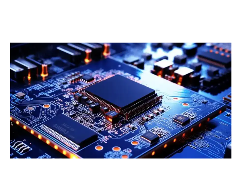
In PCBA manufacturing for 2026, precision defines market access, intelligence defines production efficiency, and green underpins long-term value.
05-19 | KingshengPCBA
In 2026, the global electronics manufacturing industry is reaching a historic inflection point, driven by simultaneous pressures on both cost and technology fronts.

05-19 | KingshengPCBA
Solder Mask Process: The Critical Procedure Determining PCB Lifespan and Reliability C - A L L E Y Home | Events | PCB | About Us | News | Contact Us Many engineers focus solely on PCB layer count, trace width, and impedance, yet often overlook the so
05-18 | KingshengPCBA
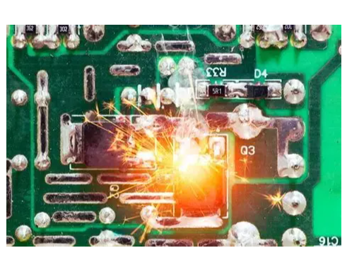
This article provides a concise, field-proven approach to eliminate wave soldering bridges—covering root causes, a three-step closed-loop solution, and a real improvement case.
05-18 | KingshengPCBA
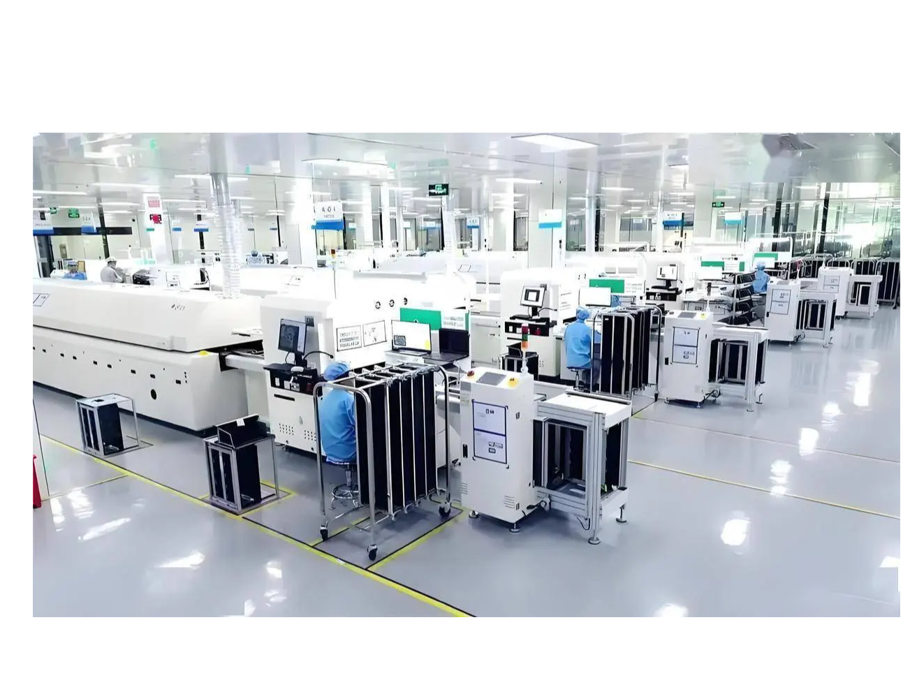
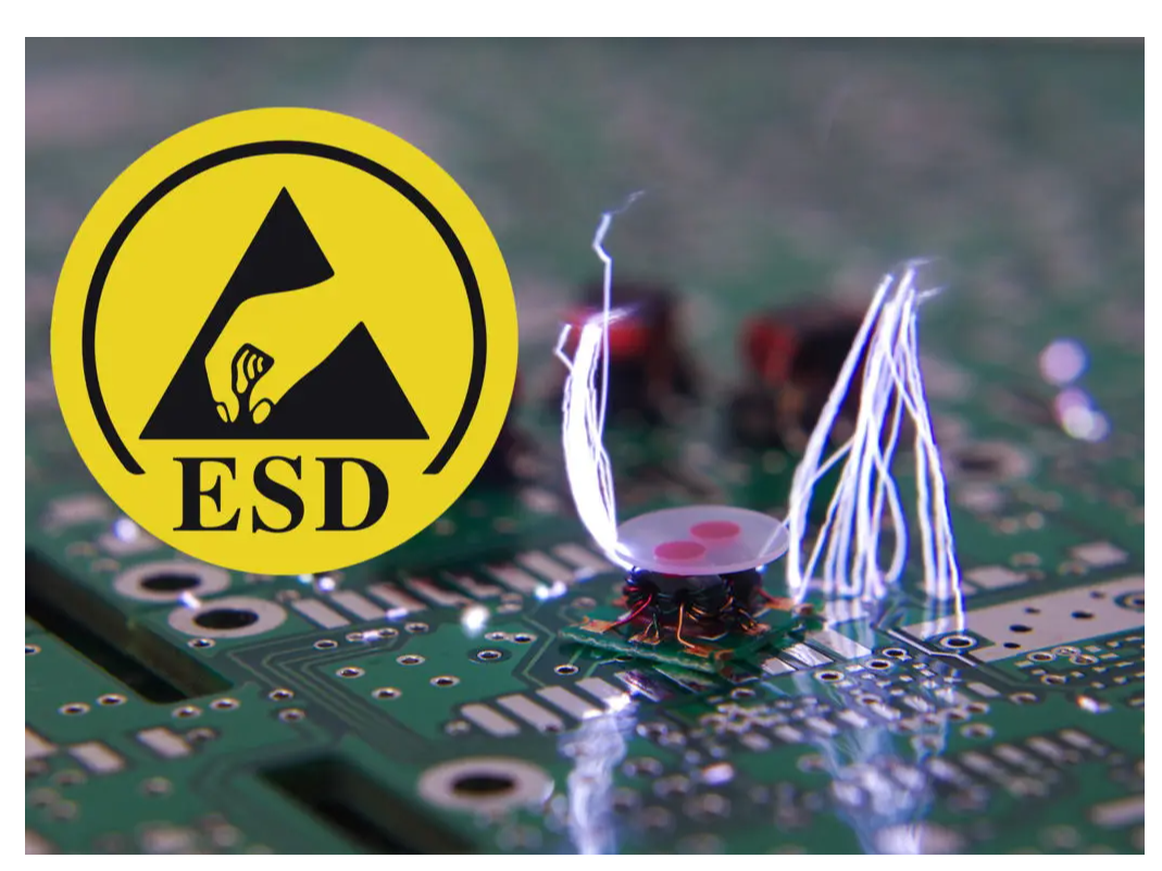
The workshop environment—specifically temperature, humidity, and electrostatic discharge (ESD) control—forms the invisible foundation that determines product reliability.

05-18 | KingshengPCBA
What exactly is impedance control, and when must it be applied? This article provides a clear, professional explanation for engineers and procurement professionals.
05-18 | KingshengPCBA
Understanding the failure mechanisms under thermal stress.
05-18 | KingshengPCBA
Two common approaches exist: customer-supplied materials (CSM) and factory-procured materials (FPM). Each has clear advantages and drawbacks. Let's understand them and help clients make informed decisions.
05-18 | KingshengPCBA
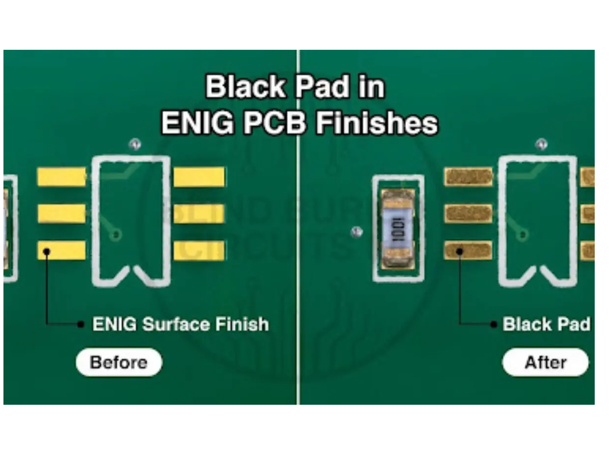
Let's break down the science and the practical countermeasures of Black Pad.
05-18 | KingshengPCBA
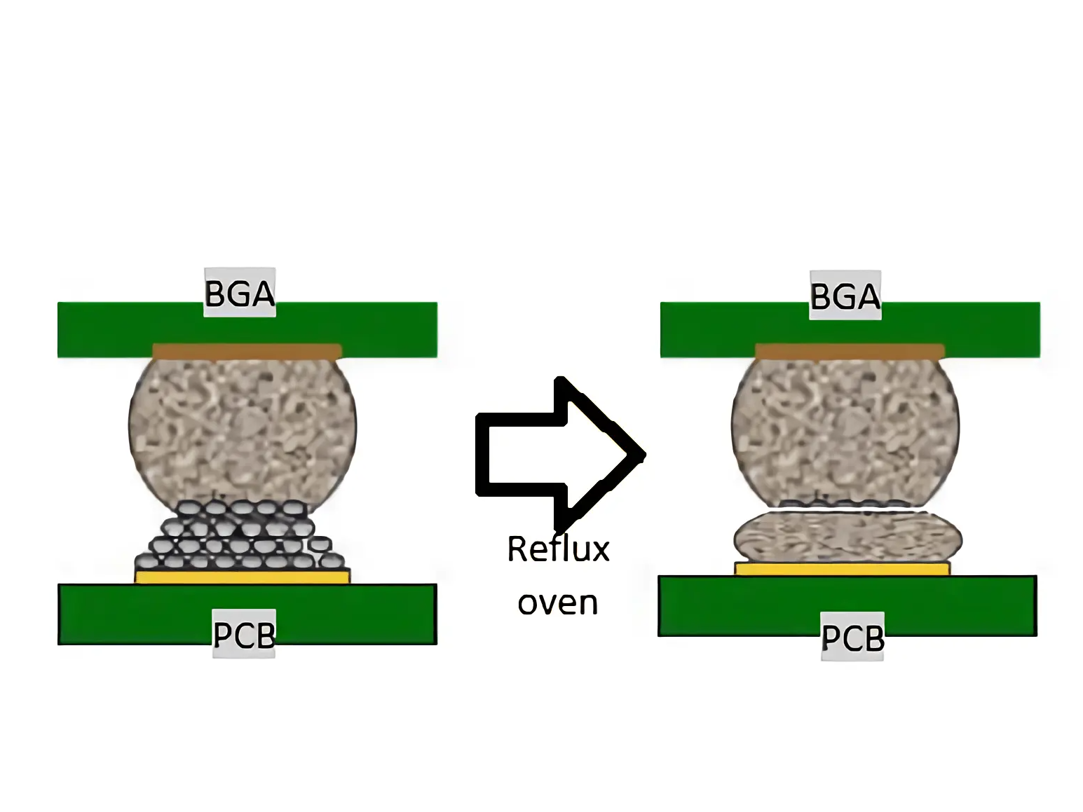
This article explains what HIP is, why it happens, and how a professional PCBA factory prevents and detects it.

05-15 | KingshengPCBA
AI demand & capacity shift drive chip price surge, impacting PCB supply chain
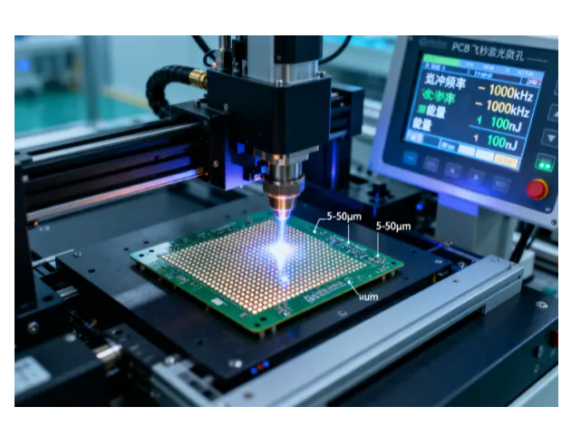
05-13 | KingshengPCBA
The key control parameters of the laser drilling process and its core advantages in HDI boards

We would also like to thank our customers for their trust and support. The company's outstanding achievements are mainly due to the loyalty of our customers, which also encourages and spurs our company to forge ahead.


