* On your first PCB Assembly order!
* Up to $300 discount
 C - A L L E Y
 Home | Events | PCB | About Us | News | Contact Us
I Introduction
Wearables, foldable phones, and medical devices are pushing PCB thickness from the standard 1.0–1.6 mm down to 0.4 mm, 0.2 mm, or even 0.1 mm. While ultra-thin PCBs (typically ≤0.5 mm) enable sleek product designs, they also introduce severe manufacturing and assembly difficulties. Many PCBA factories see first-pass yield drop to 70–85% on such boards. Understanding these challenges is the first step toward reliable, high-yield production.
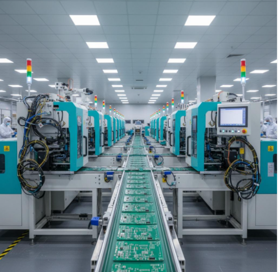
II Manufacturing Challenges: Walking a Micron Level Tightrope
1. Lamination & Warpage
When laminating multiple thin core layers (≤0.1 mm) with prepreg, the mismatch in CTE and the loss of rigidity cause slide, resin voids, and severe warpage. A 0.3 mm 4layer board can warp 0.8–1.2% after standard lamination, far above the recommended ≤0.5%.
Expert solution: Use a slow rise lamination profile (1.5–2°C/min) with peak temperature 5–10°C lower than normal; reduce pressure from 25 kg/cm² to 18–22 kg/cm² with vacuum assist; then perform hot press straightening (120°C, 15 kg/cm², 30 min) to bring warpage below 0.3%.
2. Drilling & Plating
Micro vias (≤0.15 mm) and blind vias (≤0.1 mm) require drills below 0.1 mm at spindle speeds >300k rpm. High aspect ratio micro vias also demand pulse plating with additives to achieve void free filling. Standard DC plating often leaves voids or uneven copper. Expert solution: Combine CO₂/UV laser drilling for blind vias with ultra fine mechanical drills for through holes; use reverse pulse plating to achieve >95% fill and ±2 µm thickness uniformity; perform cross section checks every shift.
3. Photo Patterning & Etching
Line/space of 50/50 µm or even 30/30 µm is common. Traditional exposure has ±15 µm alignment error – unacceptable here. Etching undercut eats into line width, while ultra thin copper foil (9–12 µm) tears easily. Expert solution: Use Laser Direct Imaging (LDI) with alignment ≤±5 µm; adopt acid etching plus micro etching to keep undercut <8 µm (etching factor >4); fix boards with carrier plates to avoid roller contact damage.
4. Solder Mask & Surface Finish
Conventional screen printed mask (20–30 µm thick) exacerbates warpage and can peel off narrow mask dams. Hot air solder leveling (HASL) instantly warps thin boards. Expert solution: Apply electrostatic spray or thin photo imageable mask (≤15 µm after cure), with minimum dam width 0.08 mm; use ENIG, ENEPIG, or ultra thin OSP – never HASL.
III Assembly Challenges: Every Component Tests Your Patience
1. Reflow Warpage
During reflow (peak 240–260°C), dynamic warpage can lift the board center >0.5 mm. This causes solder bridging, missing paste, component shift, tombstoning, and head on pillow defects.
Expert solution: Use low temperature solder paste (peak 210–220°C) with a gentle reflow profile (preheat slope ≤1.8°C/s); apply magnetic or vacuum edge holding fixtures; design anti warp copper strips or stiffeners on breakaway rails.
2. Placement Pressure “Golden Window”
Standard pick and place pressure (300–500 g for 0603 parts) easily dents a 0.2 mm board, causing pad peeling or solder extrusion. Too little pressure leads to poor wetting. Expert solution: Calibrate placement pressure specifically for ultra thin boards: 150–200 g for 01005/0201 parts, max 300 g for ICs; use soft nozzles (silicone/polyurethane); verify solder paste volume with 3D SPI before placement.
3. Rework & Depaneling
Local hot air rework often delaminates ultra thin boards or lifts pads. Mechanical routing or V scoring induces vibrations that create micro cracks, leading to hidden open circuits later. Expert solution: Preheat to 100–120°C from below, then apply micro hot air nozzle for ≤5 seconds; use UV laser depaneling (stress free, kerf ~0.1 mm); set a strict rule – scrap any board that requires more than two rework attempts.
III Why a Specialized Ultra Thin PCBA Factory Matters
An ordinary PCBA house may handle 1.0 mm boards, but ultra thin (≤0.4 mm) demands a different level of capability. A truly qualified factory offers:
Process database – parameters for dozens of materials (PI, modified FR4, Rogers) covering lamination, drilling, and reflow.
Dedicated equipment – vacuum laminators, LDI, pulse plating lines, laser routers, and vacuum reflow ovens.
Inline monitoring – real time warpage measurement, 3D SPI, 3D AOI, and Xray for closedloop control.
Failure analysis lab – to quickly identify root causes of delamination, cracks, or voids.
IV Conclusion
Ultra thin PCBs are not a simple extension of standard processes – they require systematic upgrades in materials, equipment, and skills. When your smartwatch, endoscopic camera, or satellite module must carry hundreds of components within a sub millimeter thickness, choosing the right PCBA partner is critical to product reliability.
Our PCBA factory has specialized in ultra thin boards for years, serving over 50 wearable brands with consistent SMT first pass yield above 96%. If warpage, head on pillow, or rework costs are hurting your project, contact us for a DFM review and prototype support. Make thinness a product highlight, not a production headache..
With 17 years of expertise in PCBA design, manufacturing, and service, KingshengPCBA is ready to help turn your ideas into reality. Feel free to contact us anytime to discuss your requirements and get a professional quotation.
Please send Email to kspcba@c-alley.com or call us through +86 13828766801 Or submit your inquiry by online form. Please fill out below form and attach your manufacturing files( PCB Gerber files and BOM List) if need quotation. We will contact you shortly.
 +86 13828766801
 kspcba@c-alley.com
 https://www.kingshengpcba.com/
 2/F, Building 6, Tangtou 3rd Industrial Zone, Tangtou Community, Shiyan Town, Baoan District, Shenzhen, China, 518108
We would also like to thank our customers for their trust and support. The company's outstanding achievements are mainly due to the loyalty of our customers, which also encourages and spurs our company to forge ahead.