What Defects Can AOI Detect?
 C - A L L E Y
Home | Events | PCB | About Us | News | Contact Us
In
PCBA manufacturing,
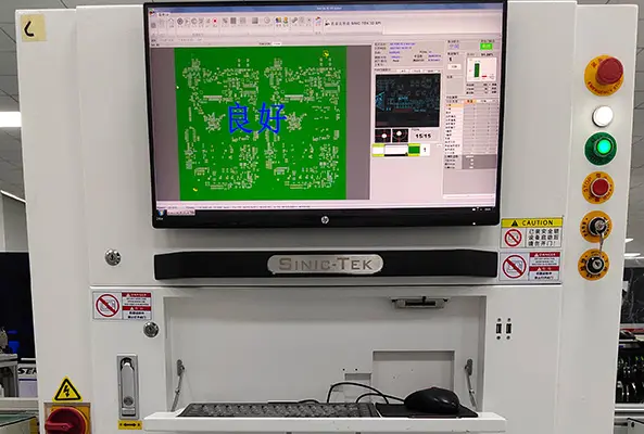
Automated Optical Inspection (AOI) is a critical quality control tool used after pick-and-place and reflow soldering. AOI uses high-resolution cameras to capture images of the circuit board and compares them against a golden template to identify various appearance and soldering defects. Below are the main defect categories detectable by AOI.
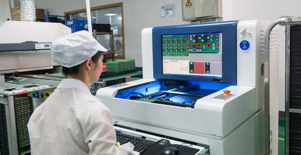 I. SMD Placement Defects
Component Missing:
I. SMD Placement Defects
Component Missing: The placement machine fails to place a component on its pad. AOI determines missing components by checking for the absence of component brightness and contour at specified coordinates.
Component Shift: The center of the component deviates from the pad center beyond the process window. AOI calculates the actual position of the component relative to the pad boundary and determines whether the X/Y offset exceeds the allowable range.
Reverse Polarity: Polarized components such as diodes, tantalum capacitors, and ICs are placed in the wrong orientation. AOI identifies polarity marks on the component surface using OCR or compares the orientation of characteristic patterns.
Tombstone: One end of a chip resistor or capacitor lifts off the pad. AOI obtains height profiles using laser or angled lighting to detect the lifted end.
Billiard / Flip: The component rests on its side or is completely flipped over. AOI checks whether the top features of the component match the template.
II. Soldering Defects
Bridging: Excess solder creates a bridge between adjacent pads. AOI detects connected bright or dark areas in the gap between solder joints.
Cold Solder / Non-wetting: Solder fails to properly wet the component termination or pad. AOI analyzes solder joint shape, solder spread area, and luster to identify shrinkage or insufficient coverage.
Insufficient Solder / Excess Solder: Solder volume deviates from the standard. AOI measures joint height and volume using 3D AOI, or estimates solder coverage using 2D shadow methods.
Solder Empty: No solder connects the component termination to the pad. AOI detects pad areas showing no solder reflection, exposing the bare pad color.
Solder Ball: Isolated spherical solder balls exist in component gaps or on the solder mask. AOI captures small, round, high-brightness objects outside pad areas.
III. Pad and PCB Substrate Defects
Pad Oxidation or Contamination: Pad color appears abnormal (darkened, blackened) or foreign material is present. AOI identifies non-copper or non-solder colors through color analysis.
Solder Mask Damage: Green solder mask is scratched, blistered, or peeled off. AOI checks solder mask uniformity and detects abnormal reflections or missing areas.
Gold Finger Contamination / Scratch: Foreign material, oxidation, or physical scratches exist on gold fingers. AOI identifies bright lines or dark spots on highly reflective surfaces.
IV. Through-hole and Connector Defects
Insufficient Solder / Incomplete Solder Penetration in Through-hole: Solder fills inadequately around the plated through-hole pin. AOI inspects the solder ring shape and coverage angle from the top or bottom side of the board.
Connector Lifted Pin: Individual pins of multi-pin connectors are not fully inserted or are floating. AOI inspects pin coplanarity and calculates height deviation for each pin.
V. Marking and Silkscreen Defects
Incorrect / Missing Character: Silkscreen characters on the PCB do not match the Bill of Materials (BOM). AOI uses OCR to read character content and compare.
Poor QR Code / Barcode Readability: Code modules have low contrast or are dirty. AOI tests read success rate and evaluates contrast parameters.
 Important Note
AOI cannot detect electrical performance defects (such as internal opens or degraded component performance) or internal voids in solder joints. For these defects, ICT, X-ray inspection, or flying probe testing is required. It is recommended that PCBA factories place AOI stations after pick-and-place and after reflow soldering, and regularly update inspection libraries to cover emerging defect types.
With 17 years of expertise in PCBA design, manufacturing, and service, KingshengPCBA is ready to help turn your ideas into reality. Feel free to contact us anytime to discuss your requirements and get a professional quotation.

 +86 13828766801
 kspcba@c-alley.com
 https://www.kingshengpcba.com/
 2/F, Building 6, Tangtou 3rd Industrial Zone, Tangtou Community, Shiyan Town, Baoan District, Shenzhen, China, 518108


