
05-29 | KingshengPCBA
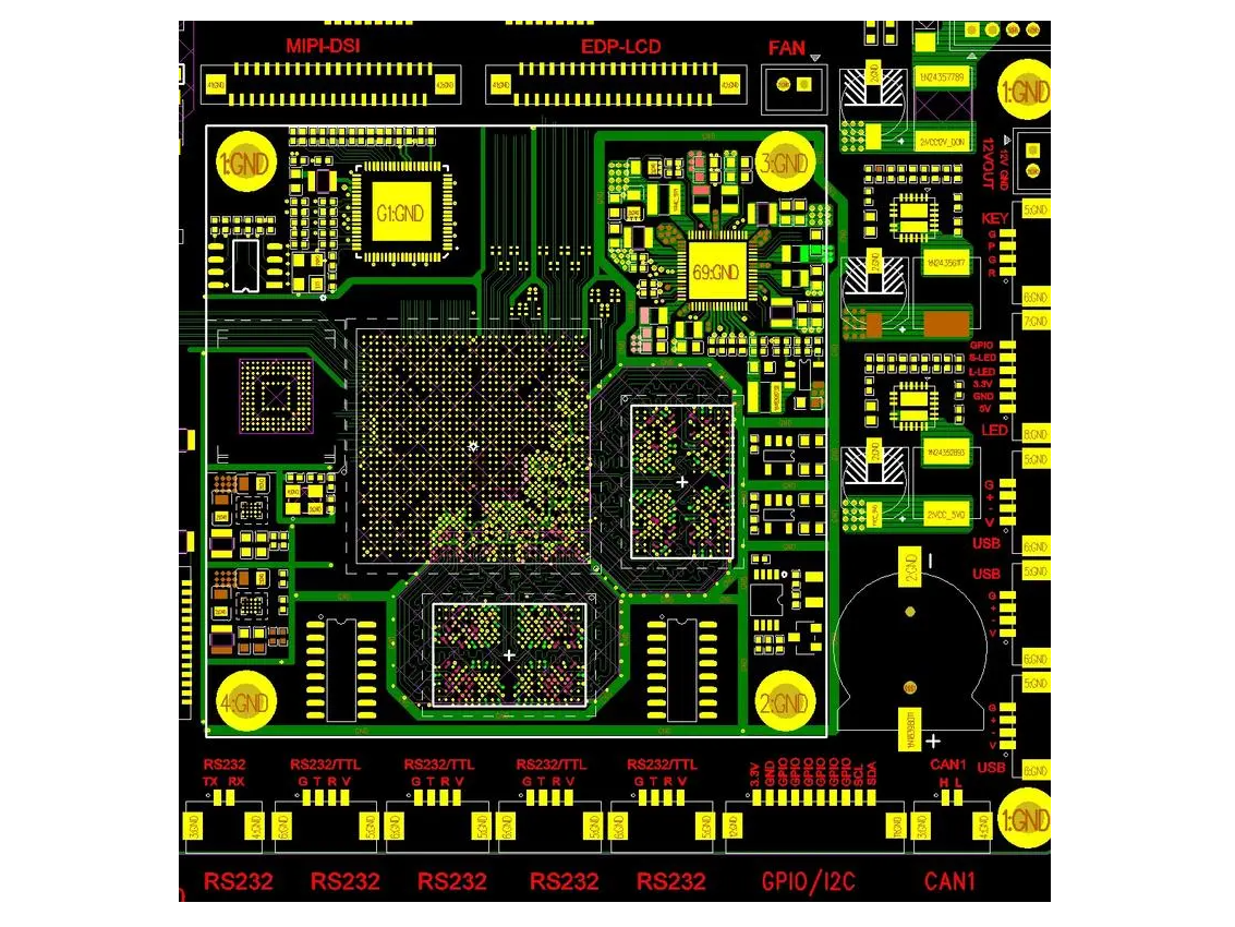
Schematic extraction in PCB reverse engineering maps physical boards to circuit diagrams, requiring verification and optimization for accuracy.
05-29 | KingshengPCBA
Four core pillars—high-multilayer, HDI, precision impedance, and high-reliability materials—are essential for industrial-grade PCB performance and long-term reliability.
05-29 | KingshengPCBA
Industrial PCBs require reinforced grounding (2–6 oz copper, -40°C to 85°C) and robust processes to withstand extreme EMI and harsh environments.
05-22 | KingshengPCBA
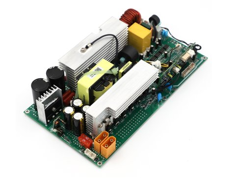
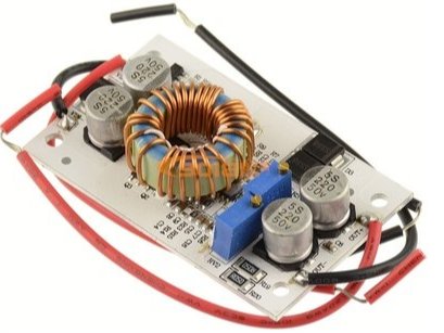
Inverter PCBAs drive clean AC power via high-efficiency conversion, robust protection & industrial-grade components for solar/backup systems.
05-22 | KingshengPCBA
Auto PCBAs ensure stable power via shock-resistant design, fast-charging circuits & automotive-grade components for vehicle safety
05-22 | KingshengPCBA
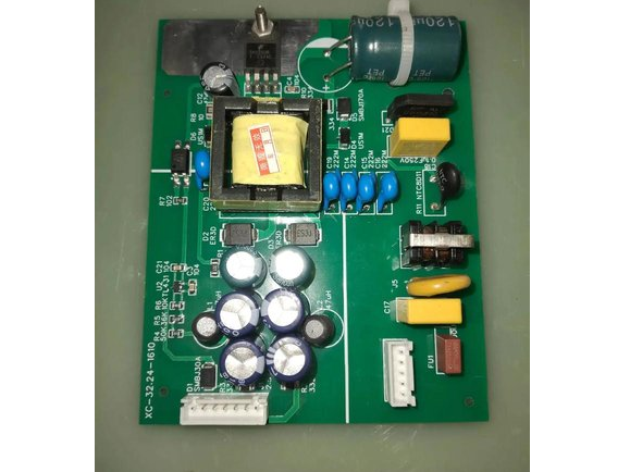
UPS PCBAs ensure stable power via precision voltage control, fast switching & robust protection for data centers/medical/industrial systems
05-22 | KingshengPCBA
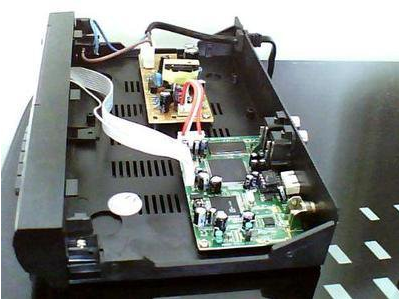
Satellite receiver PCBAs rely on precision RF design & low-loss materials for stable deep-space signal capture in harsh environments.
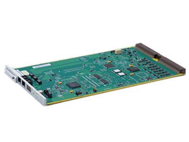
05-22 | KingshengPCBA
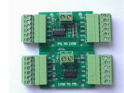
Fiber optic PCBAs enable 10G transmission via high-density, low-loss design with thermal/EMI protection, powering 5G-A/FTTR networks' reliability
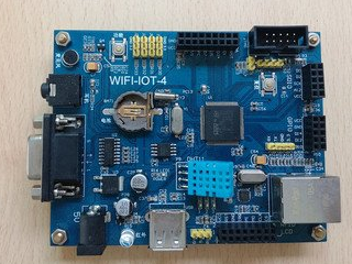
05-22 | KingshengPCBA
IoT module PCBAs require professional RF design, high-grade materials & precision SMT for stable 5G/Wi-Fi connectivity & low-power performance
05-22 | KingshengPCBA
Wireless AP PCBAs demand multi-layer RF isolation, high-TG materials & industrial-grade components for stable, high-density WiFi 6/7 coverage in harsh environments.

05-22 | KingshengPCBA
Key to fast PCB quotes: Provide complete BOM, Gerber files, specs (layers/material/finish), and flexibility for alternatives. Saves time & cost
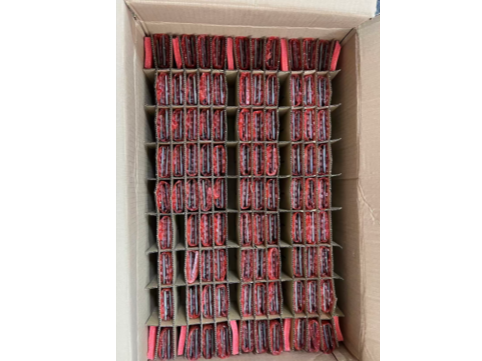
05-22 | KingshengPCBA
Gridded partition boxes ensure PCB safety during global shipping, preventing damage & building 17+ years of customer trust in AU/US/IT markets

We would also like to thank our customers for their trust and support. The company's outstanding achievements are mainly due to the loyalty of our customers, which also encourages and spurs our company to forge ahead.


