
01-10 | KingshengPCBA
1. Considering the difference between product process and storage conditions, the printed board should be used in time (recommended within 24 hours) after unpacking, and it is recommended to pre-dry before use, especially the PI substrate in
01-10 | KingshengPCBA
While in the PCB design the engineer will reserve positioning holes for printers and placement machines using. Different devices may have different requirements about positioning holes. Generally, a pair of positioning holes are required at both
01-10 | KingshengPCBA
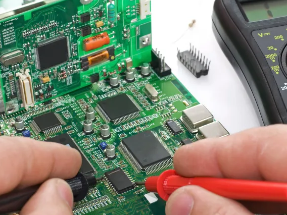
Main Tests in PCB Assembly Process-Frequently Asked Questions related to PCB assembly are those that are often tested after manufacturing. What needs to be done, however, is to design the test points when envisioned.
01-10 | KingshengPCBA
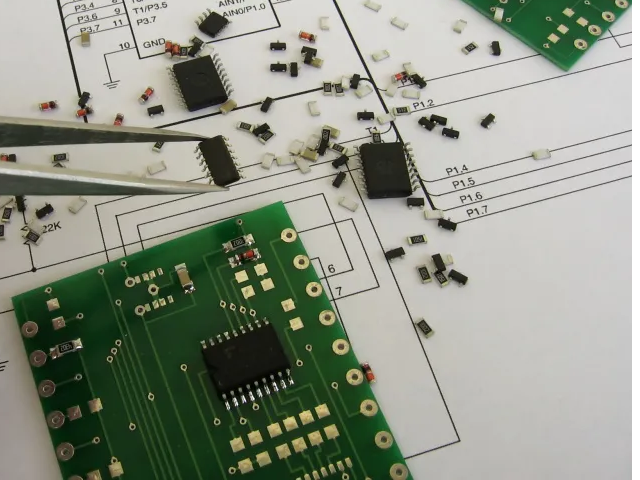
The solder paste printing process mainly solves the problem of solder paste printing volume consistency (filling and transfer), not the problem of solder paste demand for each solder joint. In other words, the solder paste printing process solves the
01-10 | KingshengPCBA
Flexible PCBs are easily deformed due to their thin and thin characteristics, so they cannot be directly assembled on SMT production lines like rigid PCBs. That is, in order to assemble the flexible PCB, the flexible PCB must be fixed on the substrate
01-10 | KingshengPCBA
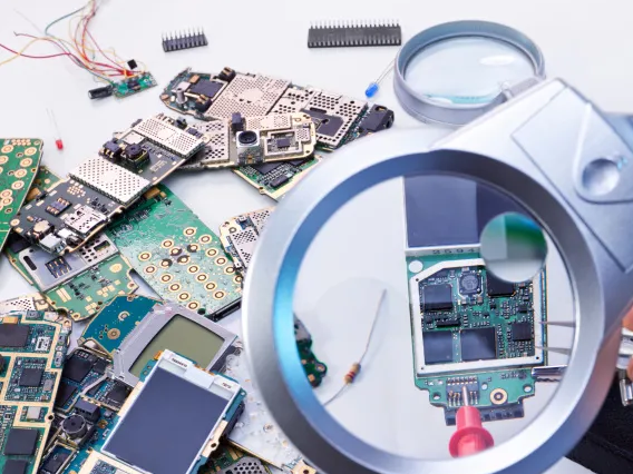
Although the recycling of electronic materials saves social resources well, there are still high risks. These refurbished materials may only deteriorate after being used for 1-2 years, because the use of materials also has a limited life time.
01-10 | KingshengPCBA
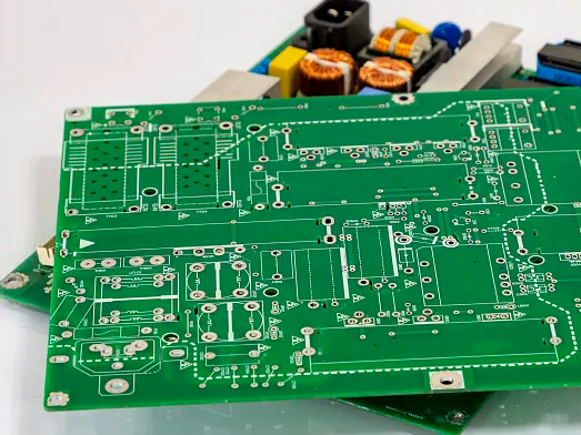
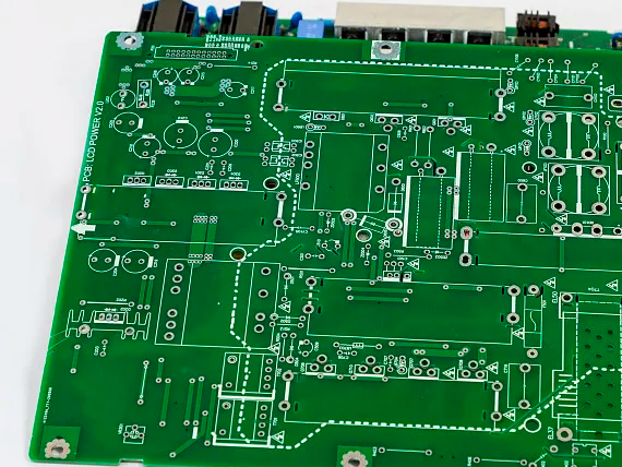
In the PCB production process, the reservation of process edges is of great significance for subsequent SMT chip processing. The process side is to increase the part of the PCB board on the two or four sides of the PCB board.
01-10 | KingshengPCBA
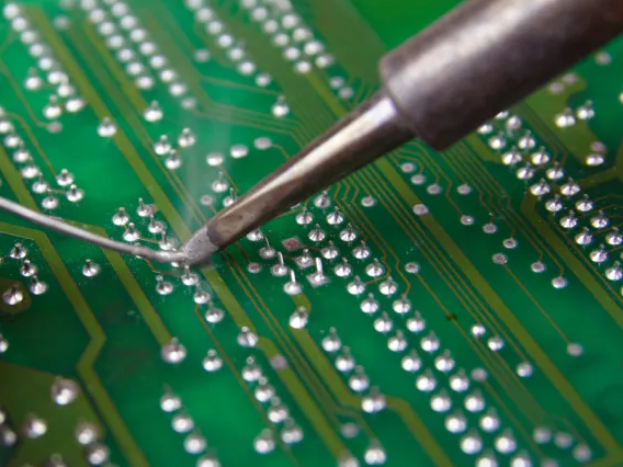
1. Wave soldering solder joint requirements: solder joints are full, shiny, not short of large area, short of tin, etc. 2. The flux spray method of wave soldering furnace is generally spray type.
01-10 | KingshengPCBA
Convene R&D, quality, business depts to hold a project meeting and discuss specific implementation plans and precautions. After the discussion, the project manager arranges the division of responsibilities of each department,
01-10 | KingshengPCBA
There are many reasons for the resistance process of the circuit board. During PCB fabrication, if the resistance is too high, it should be divided into the inner layer is too high or the outer layer is too high. In general, the reasons for operating
01-10 | KingshengPCBA
PCB circuit board impedance refers to the parameters of resistance and reactance, which hinders the alternating current. In PCB circuit board production, impedance processing is indispensable. Why should PCBA factory do impedance to the circuit board?
01-09 | KingshengPCBA
Many customers worry that the PCBA consigned cooperation method cannot strictly control the purchase of components, and worry that they are not original. In fact, solving this problem is very simple, requiring PCBA electronics manufacturers to provide

We would also like to thank our customers for their trust and support. The company's outstanding achievements are mainly due to the loyalty of our customers, which also encourages and spurs our company to forge ahead.


