01-12 | KingshengPCBA
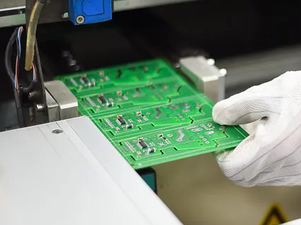
Stencil is huge critical to PCB assembly process, which directly determines the uniformity and sufficiency of every single welding pad, and then the stability of PCB after SMT assembly and reflow oven soldering.
01-12 | KingshengPCBA
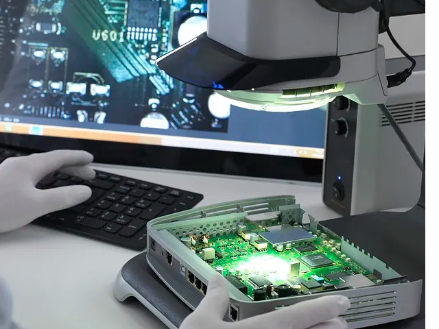
PCBA clone is always called circuit board clone, PCB reverse design or development. It is an essential technology in the electronics factory, through which you can extract PCB files and BOM list. And perfectly rebuilding it.
01-12 | KingshengPCBA
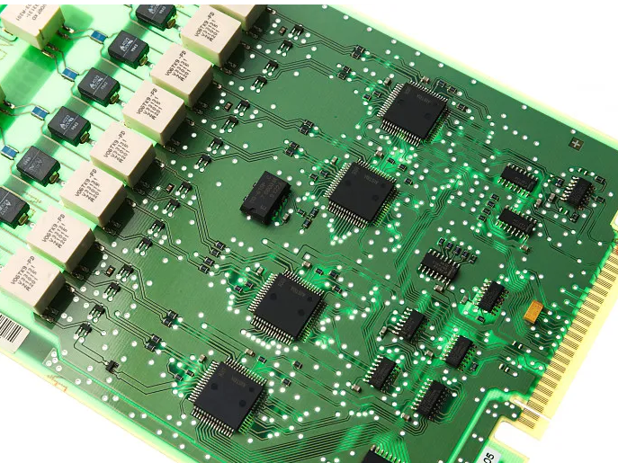
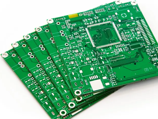
PCBs can be single-sided (one copper layer), double-sided (two copper layers on both sides of one substrate layer), or multi-layer (outer and inner layers of copper, alternating with layers of substrate).
01-12 | KingshengPCBA
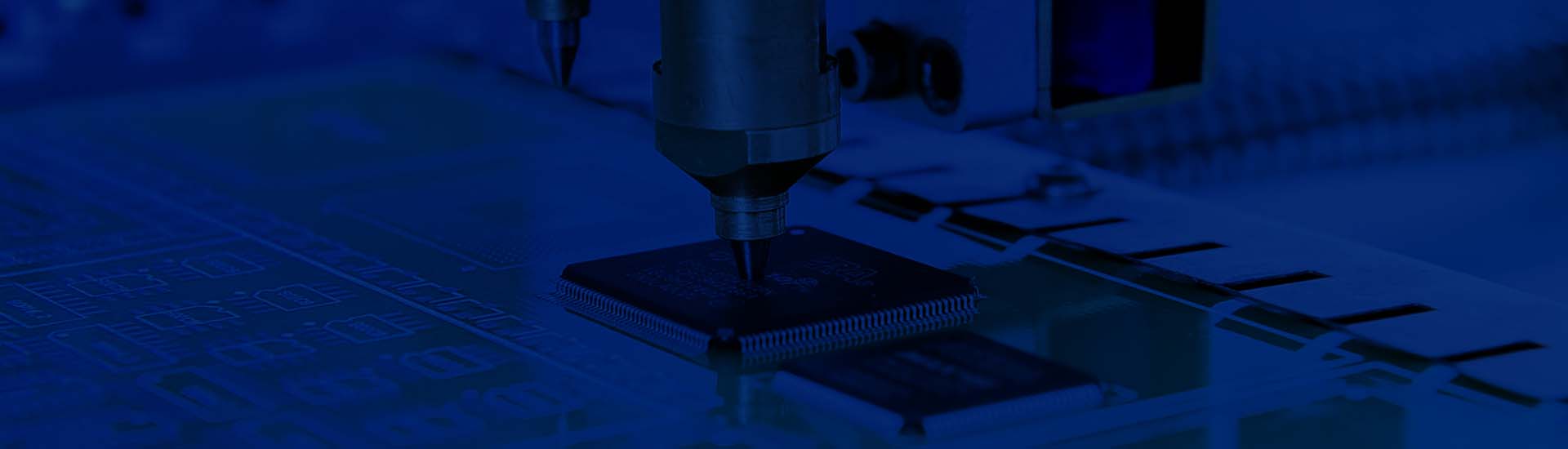
A printed circuit board (PCB) mechanically supports and electrically connects electronic components or electrical components using conductive tracks, pads and other features etched from one or more sheet layers of copper laminated onto and/or between
01-12 | KingshengPCBA
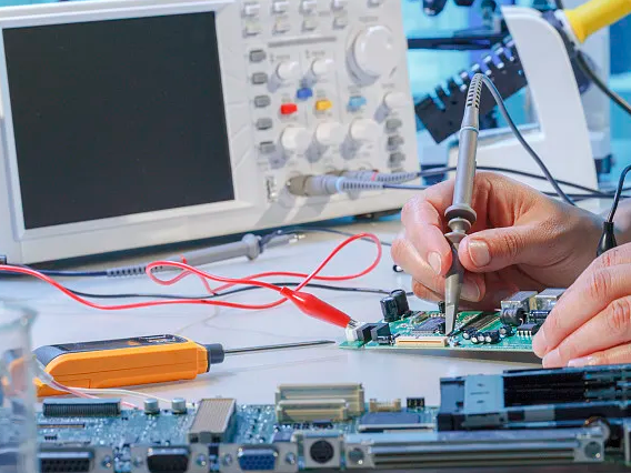
Strict incoming material inspection control and management.Never change BOM indicated material brand without customer’s permission.Standard Operation Procedure.PCB will be baked in the oven machine in advance.
01-12 | KingshengPCBA
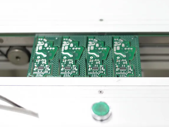
The first step of PCB assembly is applying a solder paste to the board. In a professional PCBA line, a mechanical fixture holds the PCB and solder stencil in place. An applicator then places solder paste on the intended areas in precise amounts.
01-12 | KingshengPCBA
Soldering provides reasonably permanent but reversible connections between copper pipes in plumbing systems as well as joints in sheet metal objects such as food cans, roof flashing, rain gutters and automobile radiators.
01-12 | KingshengPCBA
Laminates are manufactured by curing under pressure and temperature layers of cloth or paper with thermoset resin to form an integral final piece of uniform thickness. The size can be up to 4 by 8 feet (1.2 by 2.4 m) in width and length.
01-12 | KingshengPCBA
Copper thickness of PCBs can be specified directly or as the weight of copper per area (in ounce per square foot) which is easier to measure. One ounce per square foot is 1.344 mils or 34 micrometers thickness. Heavy copper is a layer exceeding three
01-12 | KingshengPCBA
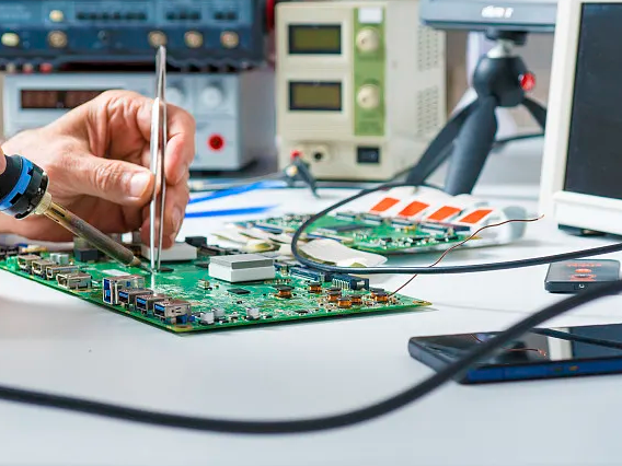
Thru-hole soldering provides stronger mechanical bonds than any other technique. Thru-hole soldering is the optimal technique for connectors, transformers, electrolytic capacitors, and other heftier circuit board components.
01-12 | KingshengPCBA
Chemical etching is usually done with ammonium persulfate or ferric chloride. For PTH (plated-through holes), additional steps of electroless deposition are done after the holes are drilled, then copper is electroplated to build up the thickness,
01-12 | KingshengPCBA
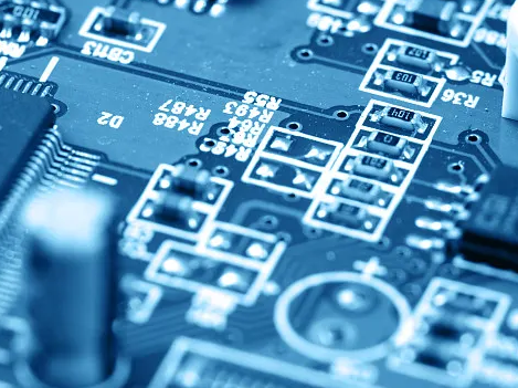
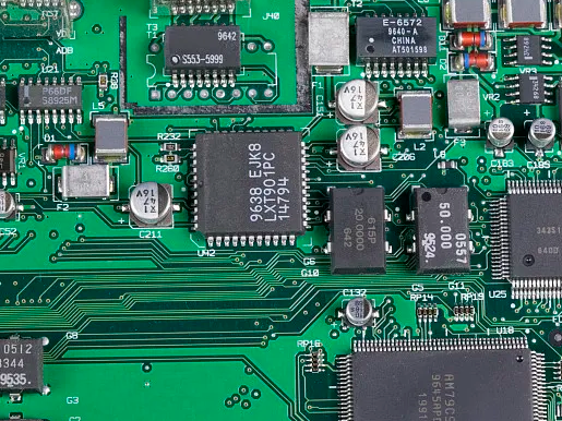
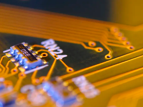
A legend is often printed on one or both sides of the PCB. It contains the component designators, switch settings, test points and other indications helpful in assembling, testing, servicing, and sometimes using the circuit board.

We would also like to thank our customers for their trust and support. The company's outstanding achievements are mainly due to the loyalty of our customers, which also encourages and spurs our company to forge ahead.


