* On your first PCB Assembly order!
* Up to $300 discount
 C - A L L E Y
 Home | Events | PCB | About Us | News | Contact Us
Why Materials Require Baking Before SMT Assembly, and how long the Baking need?
During the Surface Mount Technology (SMT) assembly process of PCBA, pre-baking certain specific materials before placement is a crucial pre-treatment step to ensure soldering quality and the long-term reliability of electronic products. The primary purpose of this step is to remove excessive moisture of these materials absorbing from the environment. This article will elaborate on the materials requiring baking, the recommended baking duration, and the scientific principles behind the baking.
Materials Requiring Baking and The Reasons
Materials requiring baking primarily fall into two main categories: Printed Circuit Boards (PCBs) and IC-type components, along with some fine-pitch components.
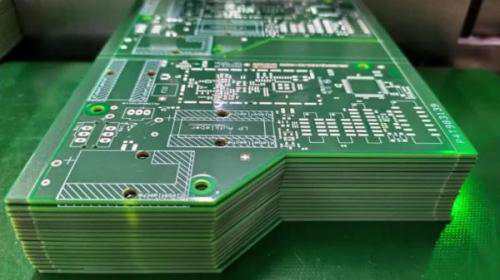
1.Printed Circuit Boards (PCBs)
Reason: PCB, as a composite material, is primarily composed of resin, fiberglass cloth, and copper foil. Its substrate (such as the commonly used FR-4) inherently possesses hygroscopic properties. During storage and transportation, the PCB gradually absorbs moisture from the surrounding environment. The moisture rapidly heats up, evaporates, and expands sharply during subsequent high-temperature processes such as reflow soldering and wave soldering, generating significant steam pressure. This can cause irreversible damage within the PCB. The most common damages are "popcorning" or "delamination," where the layers of the PCB separate and bulge. Furthermore, the escaping moisture can also lead to soldering defects, such as solder balls and voids, severely impacting product yield and long-term reliability.
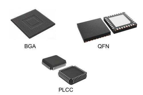
2.IC-type components and some fine-pitch components (e.g., BGA, QFN, CSP, PLCC)
Reason: These components typically use plastic packaging (epoxy resin compounds). Plastic materials are also hygroscopic. As component volume decreases and integration increases, the internal sensitivity to moisture intensifies. Under the high temperature of reflow soldering, moisture absorbed into the component interior and between the package body and the chip base will rapidly vaporize and expand. When the internal pressure exceeds the endurance limit of the packaging material, it will cause the package body to crack from the inside. This phenomenon is known in the industry as the "Popcorn Effect". These microcracks are sometimes difficult to detect immediately during E-test, potentially flowing into later stages as a hidden risk of early failure, which poses a significant threat to product quality.
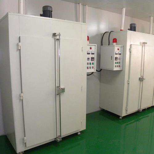
Baking Time and Condition Specifications
Baking is not performed arbitrarily; it must adhere to strict Standards (e.g., IPC-JEDEC J-STD-033) and the material manufacturer's recommendations. The core parameters for baking are temperature and time.
Baking Conditions:
Low-temperature baking: The temperature is typically 40°C ±5°C. This is suitable for components that are sensitive to temperature or require a longer dehumidification. The baking time may extend for several days (e.g., 5-9 days).
Standard/High-temperature baking: The temperature is typically 125°C ±5°C. This is the efficient baking temperature. However, it must be noted that this temperature must not exceed the PCB's Tg value (glass transition temperature, e.g., the Tg of common FR-4 is approximately 130-140°C). Otherwise, it will cause PCBs to soften and deform.
Baking Time:
For PCBs: It is generally recommended to bake at 125°C for 4-8 hours. The specific duration must refer to the recommendations of the PCB manufacturer and the PCB's thickness and layers.
For ICs and components: the baking time is solely determined by their MSL level and Floor Life. For example, if MSL Level 3 components are exposed to the environment for a period exceeding their specified Floor Life (typically 168 hours), they must be baked at 125°C for 6-8 hours before use.
General procedure: Upon material arrival, the humidity indicator card (HIC) on the packaging bag will be checked. If the indicators show moisture (e.g., circles reaching 30%, 40%, or above), or if the materials have exceeded the specified exposure time, then baking must be performed. Materials after baking should be used as soon as possible. If not fully consumed, they must be re-dried and packaged or their exposure time must be re-evaluated.
Summary
In summary, baking before PCBA placement is a critical preventive quality measure. The core reason is to prevent PCB delamination and component "popcorning" failures caused by rapid moisture vaporization during high-temperature soldering. As 16-year professional PCBA manufacturer, Kingsheng PCBA only bakes PCBs and IC components by adhering to strict Standards (e.g., IPC-JEDEC J-STD-033) and the material manufacturer's recommendations, which will significantly improving soldering yield, ultimately ensuring the quality and lifespan of electronic products, and avoiding significant economic losses due to mass quality incidents.

Please send Email to kspcba@c-alley.com or call us through +86 13828766801 Or submit your inquiry by online form. Please fill out below form and attach your manufacturing files( PCB Gerber files and BOM List) if need quotation. We will contact you shortly.
 +86 13828766801
 kspcba@c-alley.com
 https://www.kingshengpcba.com/
 2/F, Building 6, Tangtou 3rd Industrial Zone, Tangtou Community, Shiyan Town, Baoan District, Shenzhen, China, 518108
We would also like to thank our customers for their trust and support. The company's outstanding achievements are mainly due to the loyalty of our customers, which also encourages and spurs our company to forge ahead.


