* On your first PCB Assembly order!
* Up to $300 discount
 C - A L L E Y
 Home | Events | PCB | About Us | News | Contact Us
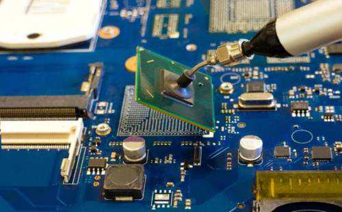
In the field of electronic manufacturing, the increasing precision of Surface Mount Technology (SMT) continuously drives process innovation. Particularly for bottom-contact components (e.g., BGA, LGA, QFN), voiding issues during the reflow soldering process have consistently been a challenging problem for the industry. Voids not only affect the thermal performance and electrical connection reliability of components but may also lead to early failures. To address this issue, the manufacturing industry has undergone a systematic evolution from stencil process improvement to the application of vacuum reflow soldering.
Root Causes of Voiding Issues
During the reflow process of bottom-contact components (e.g., BGA solder balls or LGA pads), micro-bubbles are formed and entrapped within the solder joints due to factors such as flux volatilization, uncompletely expelled gas in the solder paste, and insufficient wetting. These voids become critical defects, especially in scenarios with high thermal management requirements (e.g., processors, power devices). Traditional reflow soldering relies on hot air convection and radiant heating, but gas in molten solder is difficult to escape under atmospheric pressure, leading to persistently high voiding rates.
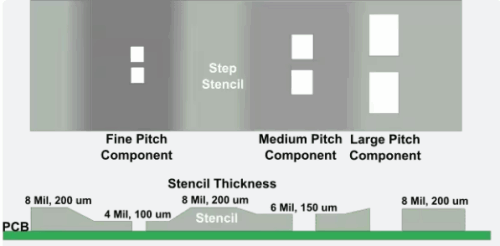
Refined Improvements in Stencil Design
The initial solution of voids focused on optimizing the stencil process. As a critical tool for solder paste deposition, stencil design directly affects solder joint quality. Through the following improvements, the voiding problem was partially mitigated:
1.Aperture design and thickness optimization: Stepped stencils (locally thinned or thickened) are used to increase solder paste volume and improve gas escaping channels; simultaneously, aperture shapes are adjusted (e.g., circular, square, or meshed) to reduce residual gas.
2.Solder paste material innovation: Use solder paste with low-volatility flux, or add antioxidants to reduce the probability of void formation.
3. Printing parameter control: Precisely control squeegee pressure, speed, and stencil release rate to ensure uniform solder paste filling and avoid void inducements.
However, while stencil improvement can reduce voids, they cannot completely eliminate the problem. Especially with the trend of component miniaturization, the physical limits of atmospheric reflow soldering gradually become apparent as solder joint sizes decrease and gas escaping space becomes restricted.
Root Causes of Voiding Issues
During the reflow process of bottom-contact components (e.g., BGA solder balls or LGA pads), micro-bubbles are formed and entrapped within the solder joints due to factors such as flux volatilization, uncompletely expelled gas in the solder paste, and insufficient wetting. These voids become critical defects, especially in scenarios with high thermal management requirements (e.g., processors, power devices). Traditional reflow soldering relies on hot air convection and radiant heating, but gas in molten solder is difficult to escape under atmospheric pressure, leading to persistently high voiding rates.
Revolutionary Breakthrough of Vacuum Reflow Soldering
The introduction of vacuum reflow soldering technology marks the transition of the void problem from "improvement" to "solution." Its core principle is that a vacuum environment is applied during the reflow process, and gases are forcibly extracted from the molten solder through negative pressure.The specific process is as follows:
1. Preheating and vacuum co-operation: During the solder melting phase (reflow zone), the vacuum level inside the oven chamber is rapidly increased to 10-100 Pa (significantly below atmospheric pressure), allowing dissolved gas to expand and escape from the solder joint.
2. Dynamic Pressure Control: The vacuum system is precisely matched with the heating profile to prevent solder splashing while ensuring gas fully expelling.
3. Post-Vacuum Cooling and Solidification: Cooling is completed in a vacuum environment to prevent gas re-dissolution.
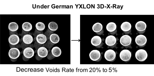
Actual data and experiment indicate that vacuum reflow soldering can reduce the void rate from 15%-25% in traditional processes to below 1%, and significantly improves solder joint mechanical strength and thermal conductivity. We (Kingsheng PCBA) made the production for a high-end aerospace products by vacuum reflow soldering for bottom-contact connector soldering, reducing the void rate from 20% to 5%.
Technical Collaboration and Future Prospects
Vacuum reflow soldering does not completely replace stencil optimization, but rather synergizes with it: precise stencil design provides a better solder paste morphology foundation for the vacuum environment, while vacuum technology compensates for the physical defects of processes in atmospheric pressure. In the future, with the surging heat dissipation requirements for 5G and AI chips, vacuum reflow soldering will gradually become the standard for high-reliability manufacturing. Concurrently, the combination of intelligent closed-loop control systems, real-time X-ray surveillance, and vacuum technology will further advance the achievement of the "zero void" goal.
From the gradual improvement of stencils to the transformative breakthrough of vacuum reflow soldering, the electronics manufacturing industry has once again demonstrated that only through foundational innovation can reliability challenges be overcome, laying a solid foundation for next-generation electronic products.

Please send Email to kspcba@c-alley.com or call us through +86 13828766801 Or submit your inquiry by online form. Please fill out below form and attach your manufacturing files( PCB Gerber files and BOM List) if need quotation. We will contact you shortly.
 +86 13828766801
 kspcba@c-alley.com
 https://www.kingshengpcba.com/
 2/F, Building 6, Tangtou 3rd Industrial Zone, Tangtou Community, Shiyan Town, Baoan District, Shenzhen, China, 518108
We would also like to thank our customers for their trust and support. The company's outstanding achievements are mainly due to the loyalty of our customers, which also encourages and spurs our company to forge ahead.


