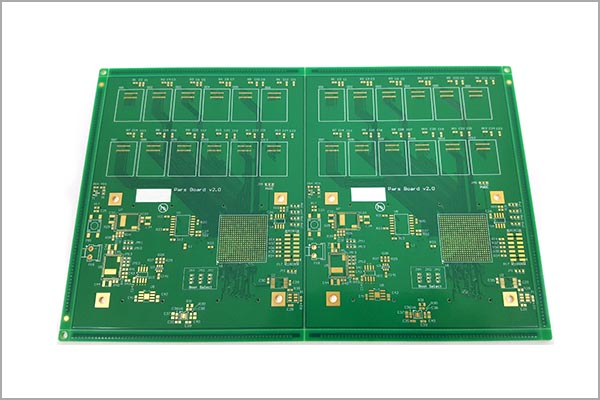
HDI (High-Density Interconnect) PCB is commonly used in applications such as smartphones, tablets, wearable devices, medical equipment, aerospace systems, and automotive electronics. KingshengPCBA(c-alley) has specialized in providing customers with advanced HDI PCB design and manufacturing techniques and high-quality products.
HDI PCB (High-Density Interconnect) PCB contains blind and/or buried vias and often contains micro vias of .006 or less in diameter. They have a higher circuitry density than traditional circuit boards.
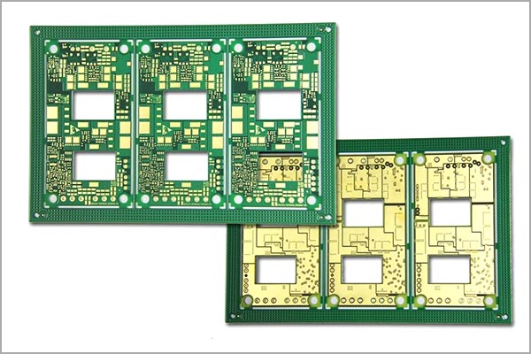
HDI PCBs are characterized by high-density attributes including laser microvias, fine lines, and high-performance thin materials. This increased density enables more functions per unit area. Higher technology HDI PCBs have multiple layers of copper-filled stacked microvias (Advanced HDI PCBs) which creates a structure that enables even more complex interconnections. These very complex structures provide the necessary routing solutions for today’s large pin-count chips utilized in mobile devices and other high-technology products.
HDI Structures: 1+N+1 – PCBs contain 1 “build-up” of high-density interconnection layers; i+N+i (i≥2) – PCBs contain 2 or more “build-up” of high-density interconnection layers.
High density: HDI PCBs use smaller vias and micro vias, allowing for increased circuit density and reduced size. This enables the placement of more components in a smaller area.
Miniaturization: HDI PCBs allow for the use of smaller and more tightly packed components, resulting in smaller and lighter electronic devices.
High-speed performance: The shorter trace lengths and reduced signal interference in HDI PCBs enable better signal integrity, making them suitable for high-speed and high-frequency applications.
Multiple layers: HDI PCBs often have multiple layers, including stacked vias and buried vias, which provide additional routing options and increased design flexibility.
Improved thermal management: HDI PCBs can incorporate thermal vias and copper-filled micro vias to enhance heat dissipation and thermal management in compact designs.
The full name of HDI is High-Density Inter-connector, it is a kind of technology (technical) for producing printed circuit boards, it uses a micro-blind buried hole technology to provide a circuit board with a relatively high distribution density, HDI is a compact product designed for small-volume users.
For the electrical requirements of high-speed signals, the circuit board must be provided with alternating current impedance control, high-frequency transmission capability, etc,multi-layering becomes a necessary design. To reduce the quality problem of signal transmission, and to cooperate with the miniaturization of an array of electronic components, the circuit boards are also constantly increasing their density to meet the demand, the emergence of assembly methods for BGA and other components has pushed printed circuit boards to an unprecedented high-density realm.
While electronic design continues to improve the performance of the whole machine, it is also trying to reduce its size. From small mobile phones to small portable products with smart products, “small” is the constant pursuit. HDI technology can make the terminal product design more compact. at the same time meet the higher standards of electronic performance and efficiency, HDI PCBs are now widely used.
Advantages of HDI PCB: increased line density is conducive to the use of advanced construction technology, better electrical performance and signal accuracy, better reliability, improved thermal properties, improved RF interference / electromagnetic interference / electrostatic discharge (RFI / EMI / ESD ), increase design efficiency, etc.
Please send Email to kspcba@c-alley.com or call us through +86 13828766801 Or submit your inquiry by online form. Please fill out below form and attach your manufacturing files( PCB Gerber files and BOM List) if need quotation. We will contact you shortly.
 +86 13828766801
 kspcba@c-alley.com
 https://www.kingshengpcba.com/
 2/F, Building 6, Tangtou 3rd Industrial Zone, Tangtou Community, Shiyan Town, Baoan District, Shenzhen, China, 518108
We would also like to thank our customers for their trust and support. The company's outstanding achievements are mainly due to the loyalty of our customers, which also encourages and spurs our company to forge ahead.


