Product Overview & Core Advantages
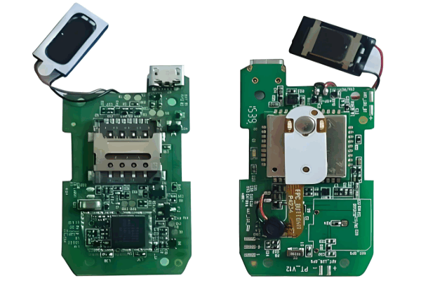
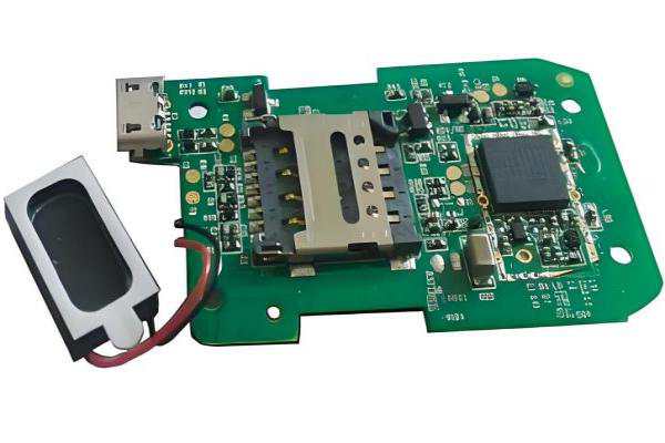
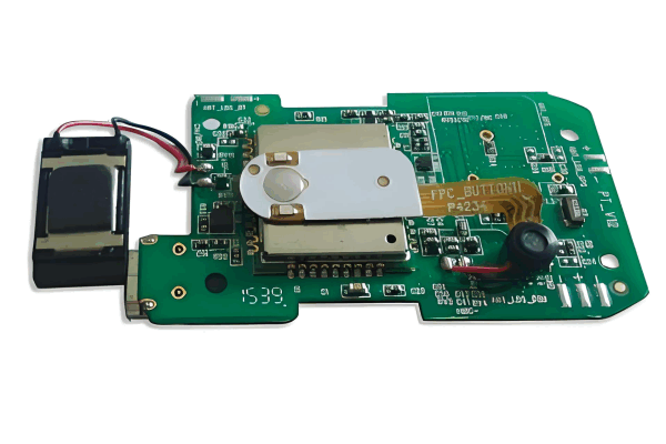
GPS Tracker PCBA (Printed Circuit Board Assembly) serves as the core component of modern tracking devices, integrating GPS modules, communication chips, microprocessors, and sensors. Our professional manufacturing delivers high-quality, reliable solutions for vehicle monitoring, asset tracking, and personal safety applications.
Key Features:
1.Substrate: FR-4 high-Tg (≥170℃) for thermal stability, Rogers RO4350B for RF circuits (εr=3.48, tanδ=0.0037)
2.Copper foil: Reverse-treated foil (Rz 3-5μm) with 1oz standard thickness (2oz for high-current paths)
3.Surface finishes:
Quality Assurance
FAQ Highlights
Conclusion: Why Choose Our GPS Tracker PCBA?
Our GPS tracker PCB assembly is designed for high precision, low power consumption, and long-term reliability. With optimized RF performance, robust material selection, and strict quality control, we ensure your tracking devices perform flawlessly in any environment.
Whether you need small-batch prototypes or mass production, our GPS tracker PCBA solutions deliver superior signal reception, energy efficiency, and durability.
Contact us today to discuss your custom GPS tracker PCB requirements!
Please send Email to kspcba@c-alley.com or call us through +86 13828766801 Or submit your inquiry by online form. Please fill out below form and attach your manufacturing files( PCB Gerber files and BOM List) if need quotation. We will contact you shortly.
 +86 13828766801
 kspcba@c-alley.com
 https://www.kingshengpcba.com/
 2/F, Building 6, Tangtou 3rd Industrial Zone, Tangtou Community, Shiyan Town, Baoan District, Shenzhen, China, 518108
We would also like to thank our customers for their trust and support. The company's outstanding achievements are mainly due to the loyalty of our customers, which also encourages and spurs our company to forge ahead.


