* On your first PCB Assembly order!
* Up to $300 discount
 C - A L L E Y
 Home | Events | PCB | About Us | News | Contact Us
Keywords: PCB stack-up, multilayer PCB design, signal integrity, EMI reduction, impedance control, PCB manufacturing
When it comes to multilayer PCB design, one critical yet often overlooked factor is the PCB stack-up. A well-optimized stack-up not only improves electrical performance but also reduces electromagnetic interference (EMI), enhances signal integrity, and balances cost and manufacturability. In this article, we’ll dive deep into what a PCB stack-up is, its design principles, common strategies, and how it influences overall circuit functionality.
PCB
What Is PCB Stack-up?
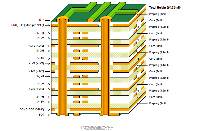
PCB stack-up refers to the arrangement of copper layers and insulating materials in a multilayer PCB. While single- and double-sided boards don’t usually require stack-up considerations, PCBs with four or more layers depend heavily on proper stack-up planning.
A typical multilayer PCB consists of:
Core layers (pre-coppered substrates)
Prepreg (pre-impregnated fiberglass sheets)
Copper foil
all laminated together based on the predefined layer configuration.
Before the layout process begins, PCB designers must decide the number of layers based on factors like circuit complexity, board size, and EMC (Electromagnetic Compatibility) requirements. This decision influences component placement, and how signal, ground, and power layers are arranged.
Key Principles of PCB Stack-up Design
Designing a proper PCB stack-up requires a multi-faceted approach:
✅ Signal Integrity
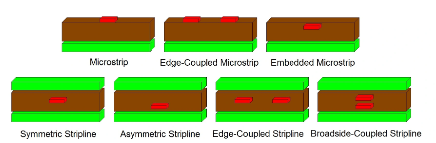
For high-speed designs, signal integrity is crucial. A recommended approach is to place signal layers between two ground planes (GND/Signal/GND), forming a stripline structure that minimizes crosstalk. For non-critical high-speed signals, microstrip routing (on outer layers adjacent to ground) may be sufficient.
⚠️ Avoid broadside-coupled stripline unless necessary. Its tight manufacturing tolerances make impedance control more difficult and less reliable.
✅ Impedance Control & EMI/EMC Shielding
Maintaining controlled impedance is critical for high-frequency signal performance. Adjacent reference planes (GND or PWR) help shield signals and reduce noise. Introducing multiple ground planes improves electromagnetic absorption.
✅ Thermal and Mechanical Considerations
Stack-up also influences heat dissipation and board warpage. Balancing layer count and symmetrical construction helps maintain board stability.
✅ Cost vs. Complexity
More layers typically mean better performance—but also higher manufacturing cost and complexity. Stack-up design should strike a balance between performance needs and production constraints.
Common PCB Stack-up Strategies
Here are two examples of 10-layer stack-up configurations, tailored for different power needs:
Single Power Plane:
S – G – S – S – G – P – S – S – G – S
Dual Power Planes:
S – G – S – S – G – P – S – S – P – S
In both cases:
"S" = Signal Layer
"G" = Ground Plane
"P" = Power Plane
Tips for stack-up optimization:
Increase spacing between certain signal layers (e.g., S1–S2) to reduce crosstalk.
Keep signal layers adjacent to ground planes whenever possible.
Use symmetrical stack-up for better thermal and mechanical performance.
PCB Stack-up
Why PCB Stack-up Matters
A carefully planned PCB stack-up directly impacts:
1. Signal Quality & EMI Reduction
Optimized layer placement reduces electromagnetic interference, enhances signal isolation, and improves power distribution quality.
2. High-Density Design
Multilayer stack-up allows more functionality in compact spaces—essential for miniaturized electronics like smartphones, IoT devices, and wearables.
3. Enhanced Noise Immunity
Insulating layers and ground planes reduce crosstalk and ground loops, ensuring stable operation in high-speed applications.
4. Reduced Transmission Delay
Shorter interconnect paths between layers lead to lower signal propagation delays, which improves performance in high-speed data transfer scenarios.
Final Thoughts
In multilayer PCB design, stack-up is not just a mechanical consideration—it’s a critical factor that affects electrical performance, thermal stability, and product reliability. Whether you're developing high-speed servers or compact IoT devices, taking time to design the right PCB stack-up will pay off in performance and durability.
Looking for a reliable PCBA partner? We specialize in high-quality multilayer PCB manufacturing and assembly, with full stack-up optimization and impedance control services.

Please send Email to kspcba@c-alley.com or call us through +86 13828766801 Or submit your inquiry by online form. Please fill out below form and attach your manufacturing files( PCB Gerber files and BOM List) if need quotation. We will contact you shortly.
 +86 13828766801
 kspcba@c-alley.com
 https://www.kingshengpcba.com/
 2/F, Building 6, Tangtou 3rd Industrial Zone, Tangtou Community, Shiyan Town, Baoan District, Shenzhen, China, 518108
We would also like to thank our customers for their trust and support. The company's outstanding achievements are mainly due to the loyalty of our customers, which also encourages and spurs our company to forge ahead.


