* On your first PCB Assembly order!
* Up to $300 discount
 C - A L L E Y
 Home | Events | PCB | About Us | News | Contact Us
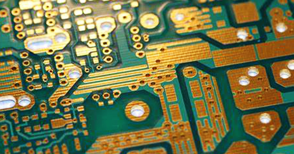
PCBA (Printed Circuit Board Assembly) processing involves connecting various electronic components on a PCB board using techniques such as surface mount technology (SMT) and through-hole technology (DIP), along with other electronic assembly processes. The primary steps in the PCBA process include SMT, automated optical inspection (AOI), DIP, functional testing (FCT), and additional procedures. Given the size variability of electronic components, different assembly techniques and requirements are necessary for each type. The assembly density of PCBA tends to be high, and the compact size and light weight of electronic products yield specific challenges and requirements in mounting. Essential factors, such as reliability, seismic resistance, and excellent solderability, dictate high standards for both the hardware and software used in PCBA processing.
The term "stamp hole" in the context of PCBA processing refers to a connection method used within the main board interface. Small boards must be interconnected to facilitate laser cutting. These connections feature small round holes located on the ribs, resembling the pits found on the edges of commemorative stamps, which we refer to as stamp holes.
The Meaning of PCBA Processing Stamp Holes
The overall design of the stamp holes closely resembles the round hole pattern cut into commemorative stamps. One significant advantage of this method is that it offers better compressive strength compared to a V-Cut. Unlike Tap technology, which requires cutting with router machines, stamp holes can be easily separated. However, a drawback is that controlling the fracture surface can be challenging. If the distance between the lines is too small, it can easily lead to damage, resulting in additional costs.
In general, PCB assembly can incorporate either stamp hole technology or dual V-shaped groove cutting technology. When opting for stamp holes, it is crucial to ensure that the stained edges are evenly distributed around each component of the PCB assembly to prevent deformation during soldering due to uneven support. The stamp hole section should be positioned close to the inner side of the PCB to prevent residual burrs from harming the assembly line after separation in panel assembly. When selecting V-shaped grooves on both sides, it is important to control the depth of the groove to be 1/3 of the total thickness (the sum of both sides). Accurate groove specifications and symmetrical depth are essential for optimal results.
Why Choose China PCBA Supplier KSPCBA as Your PCBA Processing Stamp Holes Manufacturer?
– Experienced and skilled team
– State-of-the-art equipment
– Strict quality control
– Excellent customer service
– Competitive price

Please send Email to kspcba@c-alley.com or call us through +86 13828766801 Or submit your inquiry by online form. Please fill out below form and attach your manufacturing files( PCB Gerber files and BOM List) if need quotation. We will contact you shortly.
 +86 13828766801
 kspcba@c-alley.com
 https://www.kingshengpcba.com/
 2/F, Building 6, Tangtou 3rd Industrial Zone, Tangtou Community, Shiyan Town, Baoan District, Shenzhen, China, 518108
We would also like to thank our customers for their trust and support. The company's outstanding achievements are mainly due to the loyalty of our customers, which also encourages and spurs our company to forge ahead.


