* On your first PCB Assembly order!
* Up to $300 discount
 C - A L L E Y
 Home | Events | PCB | About Us | News | Contact Us
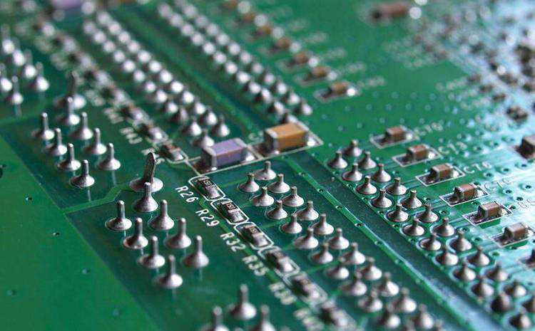
In the evolution of electronic manufacturing processes, selective wave soldering technology, by virtue of its precise and efficient characteristics, has become an indispensable key process in high-end manufacturing. Unlike the "full coverage" mode of traditional wave soldering, selective wave soldering, through program-controlled precision solder nozzles, achieves pinpoint accurate soldering, providing a perfect soldering solution for specific products.
Typical Characteristics of Applicable Products
Selective wave soldering is not suitable for all products; it primarily serves three types of typical products.
1.Mixed-technology boards, meaning that both Surface Mount Devices (SMD) and Through-Hole Technology (THT) components are on the same PCB. These boards require SMT reflow soldering to be completed first, followed by selective soldering of through-hole components, to prevent damage to already soldered components from secondary high temperatures.
2.Heat-sensitive products. In fields such as automotive electronics, aerospace, and medical equipment, products often contain temperature-sensitive components, such as sensors, connectors, or plastic joint. These components cannot withstand high temperatures above 260°C from traditional wave soldering, but the localized heating characteristic of selective soldering can effectively protect heat-sensitive components.
3.High-density boards. Modern electronic products, such as communication equipment and industrial control motherboards, have increasingly compact component and minute solder joint pitches. Traditional soldering is prone to bridging, whereas the precise soldering of selective wave soldering can effectively prevent this issue, ensuring welding quality.
Value of Technical Advantages
The core value of selective wave soldering is primarily reflected in quality improvement. By precisely controlling solder volume, soldering time, and temperature, optimal soldering results are achieved for each solder joint, and solder joint consistency is significantly superior to traditional processes. Statistically, the adoption of selective wave soldering can reduce the soldering defect rate by over 60%.
In terms of cost control, although the equipment investment for this technology is high, the comprehensive benefits are significant. Solder consumption is reduced by 30%-50%, subsequent repair costs are lowered, and first pass yield is increased. It’s particularly suitable for small to medium batch, multi-variety production models. For high-value military, medical, and automotive electronic products, the benefits brought by quality improvement far exceed the equipment investment.
More importantly, selective wave soldering enhances design flexibility. Engineers are not required to compromise designs due to process limitations; they can freely adopt components with different package forms, promoting product development towards higher performance and smaller size. This improvement in design freedom provides solid technical support for product innovation.
Future Development Trends
With the rapid development of emerging industries such as 5G communication, new energy vehicles, and artificial intelligence, higher requirements are placed on electronic manufacturing processes. Selective wave soldering technology is evolving towards intelligentization and flexibility, deeply integrating with Industry 4.0 and smart manufacturing, to further optimize process parameters and improve production quality and efficiency through data acquisition and analysis.
Selective wave soldering represents not only a technological advancement but also an evolution in manufacturing philosophy. It reflects a electronic manufacturing shift from extensive to precision-focused production, and from mass manufacturing toward customization.
At Kingsheng PCBA, we are committed to pursuing higher quality and enhanced reliability in electronic manufacturing. The adoption of advanced selective wave soldering equipment marks a key step in our transition toward producing higher-end circuit boards. We are dedicated to providing robust technical support for the development of higher-value electronic products.

Please send Email to kspcba@c-alley.com or call us through +86 13828766801 Or submit your inquiry by online form. Please fill out below form and attach your manufacturing files( PCB Gerber files and BOM List) if need quotation. We will contact you shortly.
 +86 13828766801
 kspcba@c-alley.com
 https://www.kingshengpcba.com/
 2/F, Building 6, Tangtou 3rd Industrial Zone, Tangtou Community, Shiyan Town, Baoan District, Shenzhen, China, 518108
We would also like to thank our customers for their trust and support. The company's outstanding achievements are mainly due to the loyalty of our customers, which also encourages and spurs our company to forge ahead.


