* On your first PCB Assembly order!
* Up to $300 discount
 C - A L L E Y
 Home | Events | PCB | About Us | News | Contact Us
In the high-stakes arena of electronics manufacturing, while engineers obsess over component selection and test strategies, one unsung hero silently dictates up to 60% of SMT defects: The humble solder paste stencil. Choose wrong, and you’ll battle bridging, insufficient joints, and tombstoning. Choose wisely, and you unlock near-zero-defect production. Here’s how industry leaders engineer perfection at the micron level.
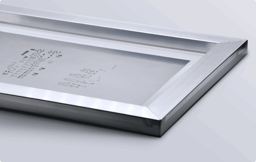
PCBA Stencil
1. Material Revolution : Beyond Basic Stainless Steel
Not all stencils are created equal. The material directly impacts paste release, durability, and cost:
| Material Type | Thickness Range | Best For | Lifespan |
| Standard 304SS | 100-150μm | Low-density boards | 50k impressions |
| Electroformed Nickel | 50-130μm | Ultra-fine pitch(<0.3mm BGA) | 100k+ |
| Nano-Coated Steel | 80-150μm | Lead-free pastes, QFN |
150k+ |
Case Study: A drone manufacturer reduced bridging defects by 73% after switching to nano-coated stencils for their 0.25mm pitch IMU chips. The non-stick surface achieved near-100% paste release vs. 85% on standard steel.
2. Thickness Calculus: The 1:1 Rule Isn’t Enough
While the classic "stencil thickness = ball diameter" guideline works for simple designs, modern mixed-technology boards demand precision engineering:
01005 Components: 60-80μm thickness
0.3mm Pitch BGA: 100-120μm
Power Connectors: 150-200μm (requires step-down zones)
Press-Fit Holes: 0μm (etch relief areas)
Pro Tip: Use solder paste volume calculators like KIC Solder to model
3. Laser vs. Electroformed: Cutting Through the Hype
Laser-Cut Stencils (Industry Standard)
Pros: Fast turnaround (<24hrs), ±5μm accuracy, cost-effective
Cons: Micro-burrs require electropolishing (adds $80-150)
Best for: Prototypes to mid-volume production
Electroformed Stencils (Premium Solution)
Pros: Smooth sidewalls (Ra<0.1μm), no post-processing, ideal for <0.3mm pitch
Cons: 3-5x cost, 3-day lead time
Best for: Medical/Aerospace HDI boards
Data Insight: Electroformed stencils achieve 99.2% paste transfer vs. 95.7% for laser-cut (per IPC-7525B).
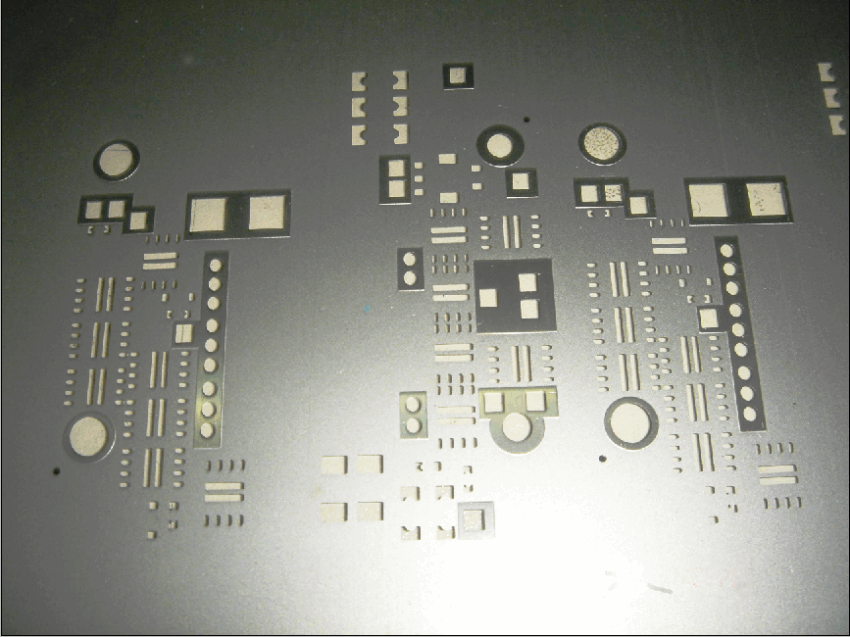
PCBA Stencil
4. Aperture Design: Geometry is Everything
Avoid "copy-paste" footprints. Optimize shapes per component:
| Component | Optimal Aperture Design | Area Ratio |
| 0402 Resistors | Home-plate shape (reduces tombstoning) | >0.66 |
| QFN Center Pad | 60% coverage + cross-stitch vents | >0.50 |
| µBGA | Circular with 1:1 ratio | >0.70 |
Critical Ratios:
Area Ratio = (L x W) / [2(L + W) x T] ➔ Must be >0.66
Aspect Ratio = Width / Thickness ➔ Must be >1.5
5. Step Stencils: Solving Mixed-Technology Nightmares
When boards combine 01005 chips and 12mm tantalum capacitors, single-thickness stencils fail. The solution:
Step-Up: Add 50-100μm thickness over large component areas
Step-Down: Etch away 30-50μm for fine-pitch regions
Process Control: Laser welding ensures step height accuracy ±5μm
Real-World Impact: An automotive module maker eliminated 98% of voiding in MOSFET pads using step-down stencils, reducing thermal resistance by 40%.
6. Nano-Coatings: The Secret Weapon for Lead-Free Pastes
As SAC305 pastes dominate, their poor wettability demands surface engineering:
PTFE-Based Coatings: Reduce paste adhesion by 70%
Electroless Nickel: Hardness >500 HV prevents wear
Gradient Coatings: Multi-layer stacks for >500k impressions
ROI Analysis: At $250 per coating, 4x lifespan extension delivers 300% ROI.
7. Inspection & Maintenance: Don’t “Set and Forget”
A stencil’s performance degrades with every wipe. Implement:
Laser Inspection: Scan for aperture wear >±8μm deviation
Tension Monitoring: Maintain 35-50N/cm² (IPC standard)
Automated Cleaning: 90% IPA + vacuum drying every 5 prints
Cost of Neglect: A worn stencil caused $220k rework at a contract manufacturer due to 18% solder volume drop.
The Stencil Selection Matrix: Match Technology to Need
| Your Challenge | Optimal Solution | Cost Impact |
| Prototyping mixed boards | Laser-cut + electropolishing | $$ |
| Ultra-fine pitch (<0.3mm) | Electroformed nickel | $$$$ |
| High-volume QFN production | Nano-coated step stencil | $$$ |
| Low-mix, high-reliability | Standard steel + IPC-7525B design | $ |
Why Top Tier EMS Providers Never Compromise on Stencils?
A study across 5 electronics factories revealed:
“Stencil-driven defects account for 58% of first-pass SMT failures”
The 1% Rule: A 1% improvement in paste volume consistency reduces reflow defects by 8%
Speed Multiplier: Optimized stencils enable 50% faster line speeds by eliminating print inspections
Material Savings: Precision apertures cut paste consumption by 22% annually
The Invisible Precision Art
In the symphony of SMT manufacturing, the stencil is the conductor—unseen but orchestrating every note of quality. While engineers chase exotic components and AI-driven testers, masters of the craft know: Perfection begins with 100 microns of perfectly released solder paste.
Your stencil isn’t a commodity; it’s the foundation of your first-pass yield. Treat it as the precision instrument it is, and watch defects vanish, throughput soar, and customers marvel at your quality.
“The difference between good and great PCBA? Look through the stencil.”

Please send Email to kspcba@c-alley.com or call us through +86 13828766801 Or submit your inquiry by online form. Please fill out below form and attach your manufacturing files( PCB Gerber files and BOM List) if need quotation. We will contact you shortly.
 +86 13828766801
 kspcba@c-alley.com
 https://www.kingshengpcba.com/
 2/F, Building 6, Tangtou 3rd Industrial Zone, Tangtou Community, Shiyan Town, Baoan District, Shenzhen, China, 518108
We would also like to thank our customers for their trust and support. The company's outstanding achievements are mainly due to the loyalty of our customers, which also encourages and spurs our company to forge ahead.


