* On your first PCB Assembly order!
* Up to $300 discount
 C - A L L E Y
 Home | Events | PCB | About Us | News | Contact Us
What is the most troublesome part of PCB design for you every time? Is it the dense wiring? Or the frustrating EMI issues? The root of the problem may be hidden in a place you can't see—the PCB stack-up structure.
When your design transitions from small-batch laboratory production to mass production, have you ever encountered a sudden deterioration in signal integrity? When the product's operating temperature rises, does the PCB experience unexpected failures? These pain points are very likely due to unreasonable stack-up design.
As we face increasingly high-speed circuit designs, a reasonable stack-up structure has become one of the key factors in project success or failure.
Why is PCB stack-up design so critical?
When choosing a stack-up structure, you need to balance four key factors: product complexity, signal speed, EMC requirements, and cost budget.
Here are the three core performance aspects it directly impacts:
1. Signal Integrity
High-speed signal layers need to be sandwiched between power or ground planes to form a stripline structure. For example, when the 3rd layer is used as a high-speed signal layer, ground planes need to be set above and below it.
2. Electromagnetic Compatibility (EMC)
A reasonable stack-up structure can reduce crosstalk by more than 60%. Multiple ground plane layers can effectively reduce PCB impedance and lower common-mode EMI.
3. Mechanical Stability
The stack-up must remain symmetrical; otherwise, differences in thermal expansion and contraction will cause the board to become a "curved screen," leading to a sharp decline in soldering yield.
PCB Stack-Up Design Pitfall Avoidance Guide
PCB Stack-Up Scheme Selection for Different Application Scenarios
1. Double-Layer Boards: The Cost of a Low-Cost Solution
Suitable for applications with simple structures and low signal rates, such as home appliance controllers and LED driver boards.
Significant cost advantages but poor EMC performance, susceptible to signal interference, and not suitable for complex wiring.
Design Tip: Where space permits, maximize ground plane area to create a local reference plane.
2. Four-Layer Board: A Cost-Effective Choice
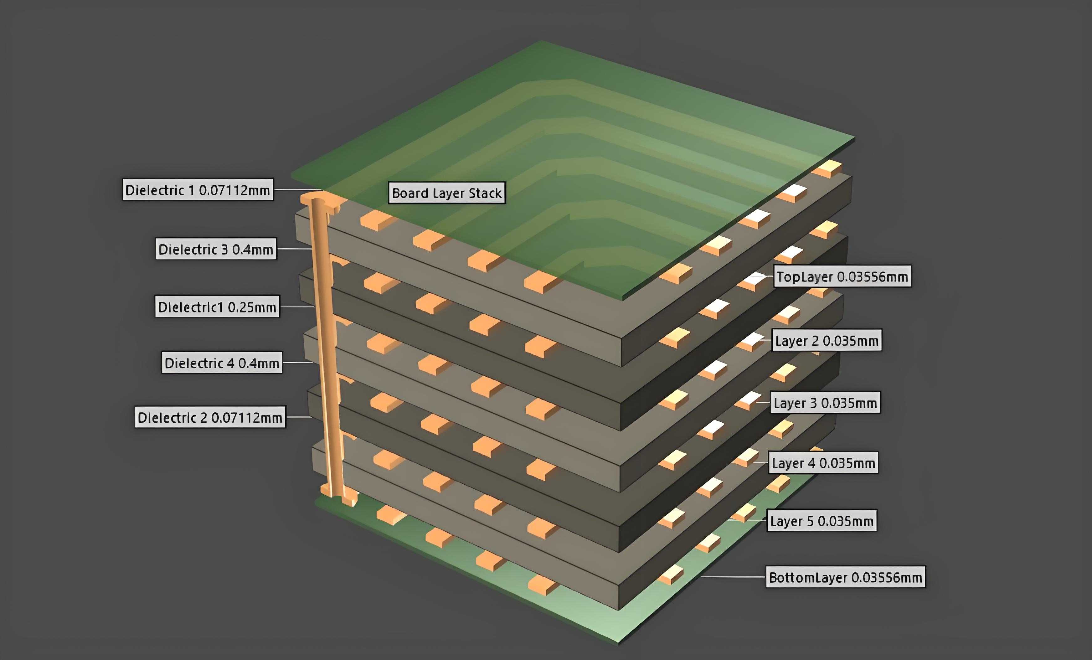
For common medium-complexity applications such as MCU development boards and industrial control boards, a four-layer board is the optimal choice. Classic structure: TOP (Signal)-GND-PWR-BOTTOM (Signal).
The advantage is that the signal layer is close to the reference ground layer, which can effectively control impedance and reduce the length of the signal return path. Suitable for digital circuit designs with differential signals or higher frequencies.
Advanced Tip: When the power layer and ground layer are adjacent, controlling the interlayer dielectric thickness to 0.1-0.2mm can reduce the power plane impedance.
3. Six-Layer Boards: A Haven for High-Speed Signals
When encountering a large number of high-speed signals (such as DDR4, PCIe), or when the board size is small and the wiring density is high, a six-layer board is a better choice.
Recommended structure: TOP-GND-Signal1-PWR-GND-Signal2-BOTTOM. This architecture sandwiches the high-speed signal layer (Signal1) between double ground planes, providing the best EMI suppression effect.
Cost Warning: Each additional layer may increase the cost by 50%, but the EMI risk can be reduced by 30%.
4. Eight Layers and Above: The Ultimate Solution for High-Density Designs
Suitable for high-complexity BGA packages or ultra-high-speed systems. Typical scheme: TOP-GND-Signal1-PWR-GND-Signal2-PWR-BOTTOM, with four signal layers and four reference planes.
For harsh environments such as automotive electronics, select Tg≥180℃ material to improve the reliability of the PCB by 30%+ under -40℃~150℃ temperature cycling.
5. Impedance Control is the Lifeline of High-Speed Design
Precision Control: Use UV laser direct imaging (LDI) technology, with a line width tolerance of ±0.2mil
Manufacturing Compensation: 1oz copper thickness is actually counted as 1.2mil in the model
Special Laminates: When Rogers and FR4 are mixed, use materials with the same coefficient of thermal expansion in symmetrical positions
6. Design for Manufacturability to Avoid Mishaps
PP Sheet Selection: No more than 3 PP layer stacks per dielectric layer
Thickness Control: PP dielectric thickness between two layers ≤21mil (excessive thickness leads to processing difficulties)
Copper Foil Selection: 0.5oz copper foil is preferred for the outer layer, and 1oz for the inner layer; the power layer is selected according to current requirements (2-3oz)
PCB Stack-Up Design Pitfall Avoidance Guide
Practical Tips in Manufacturing Process
1. Foil vs Core Stacking Method
Foil method (copper foil pressed on the outer layer): low cost, but difficult to control impedance (surface resin flow problem)
Core method (core board for the outer layer): 20% higher cost, but high impedance accuracy
2. Mixed Material Lamination
When Rogers and FR4 are mixed, a stepped lamination process must be adopted to prevent interlayer slippage
3. Thick Copper Board Manufacturing
Copper layers above 3oz adopt differential etching process - first etch to 2oz, and then pattern to the target thickness
Key Step After Design Completion: Verifying the Stack-up
After the stack-up design is completed, how to verify it?
1. Impedance Verification
Ensure impedance tolerance is controlled within ±10% by considering various production factors.
2. Design Analysis
Detect potential design hazards, eliminate production difficulties and design defects, and alert factors affecting price.
3. Stack-up Verification
Match stack-up structures that meet production requirements to ensure the reliability of multilayer PCBs.
4. Document Comparison
Compare the differences between previous and current stack-up versions to avoid oversights.
KingSheng PCBA is a company that specializes in PCB assembly services. We offer turnkey solutions for electronic manufacturing services, including PCB design, fabrication, and assembly. Our professional application engineers, skilled and trained in KingSheng for over 10 years, are here to offer you 24/7 technical support.

Please send Email to kspcba@c-alley.com or call us through +86 13828766801 Or submit your inquiry by online form. Please fill out below form and attach your manufacturing files( PCB Gerber files and BOM List) if need quotation. We will contact you shortly.
 +86 13828766801
 kspcba@c-alley.com
 https://www.kingshengpcba.com/
 2/F, Building 6, Tangtou 3rd Industrial Zone, Tangtou Community, Shiyan Town, Baoan District, Shenzhen, China, 518108
We would also like to thank our customers for their trust and support. The company's outstanding achievements are mainly due to the loyalty of our customers, which also encourages and spurs our company to forge ahead.


