* On your first PCB Assembly order!
* Up to $300 discount
 C - A L L E Y
 Home | Events | PCB | About Us | News | Contact Us
(A) layout planning
In PCB design, layout is the first step and a crucial step. To fully consider the function of the components, heat dissipation, signal interference and other factors. For example, large heat-generating components should be as close as possible to the heat sink, such as the CPU, etc.; sensitive components should be away from sources of interference, such as crystal near the signal lines should be avoided to avoid arranging vulnerable to interference. At the same time, we should reasonably plan the placement of components, so that the line connection is the shortest and most concise, reducing the delay and loss of signal transmission.
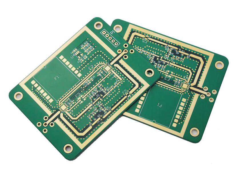
PCB
(B) Wiring principles
Wiring needs to follow certain rules to ensure signal integrity and stability. For high-speed signals, attention should be paid to line length matching, impedance matching, to prevent signal reflection and distortion. Generally speaking, high-speed signal lines should be as short and straight as possible, avoiding right-angle turns, and 45-degree angles or arc turns can be used. In addition, the isolation between different signals should be considered to prevent crosstalk, such as analog and digital signals should be wired separately .
Why Choose China PCBA Supplier KSPCBA as Your Manufacturer?
– Experienced and skilled team
– State-of-the-art equipment
– Strict quality control
– Excellent customer service
– Competitive price

Please send Email to kspcba@c-alley.com or call us through +86 13828766801 Or submit your inquiry by online form. Please fill out below form and attach your manufacturing files( PCB Gerber files and BOM List) if need quotation. We will contact you shortly.
 +86 13828766801
 kspcba@c-alley.com
 https://www.kingshengpcba.com/
 2/F, Building 6, Tangtou 3rd Industrial Zone, Tangtou Community, Shiyan Town, Baoan District, Shenzhen, China, 518108
We would also like to thank our customers for their trust and support. The company's outstanding achievements are mainly due to the loyalty of our customers, which also encourages and spurs our company to forge ahead.


