* On your first PCB Assembly order!
* Up to $300 discount
 C - A L L E Y
 Home | Events | PCB | About Us | News | Contact Us
Amidst the pursuit of high speed and high frequency in modern electronic equipment, the precision of tiny holes on printed circuit boards (PCBs) has become a critical factor impacting signal integrity. Back drilling technology is a precision process engineered to address this challenge. It creats a cleaner transmission path for high-speed signals by removing unnecessary metal stubs in vias.
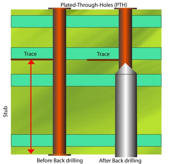
Back drilling, as its name implies, is a secondary drilling from the backside of the PCB. In traditional PCB manufacturing, vias are used to connect circuits among different layers. These holes are formed into a metalized hole wall that penetrates the entire thickness of the board after electroplating. However, in high-speed and high-frequency applications, these metal stubs in vias can act like antennas, leading to signal reflection, attenuation, and crosstalk—this is known as the "Stub Effect." Back drilling uses specialized drill bits to precisely remove metal stubs in signal vias that are not used for connection with cables, only retaining the necessary interconnection segments, thereby eliminating the negative effects caused by these superfluous metal stubs.
Why is such a precise process required? The answer lies in the characteristics of high-frequency signals. When signal frequency reaches the GHz level, any impedance discontinuity will cause signal distortion. Superfluous via stubs act like sharp turns on a highway, significantly reducing the signal's "speed". Studies have shown that under a 10GHz frequency, a only 1.5mm stub can cause insertion loss of tens of decibels. By back-drilling to keep the stub length to within 0.2mm, this loss can be reduced by over 80%, significantly improving signal integrity.
This process is crucial for modern electronic equipment such as 5G communication equipment, high-performance computing servers, and high-speed network switches. In these devices, differential signals are transmitted at tens of gigabits per second, and any signal distortion can lead to increased data error rates or even system failure. Back-drilling technology enables high-speed transmission of 28Gbps or even 56Gbps, serving as the underlying support for realizing next-generation communication technologies.
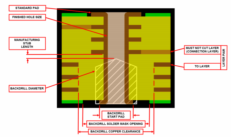
Achieving precise back-drilling faces numerous challenges: precise control of drilling depth is required to avoid damaging the functional hole walls; the drilling characteristics of different materials must be considered; and hole wall smoothness must be ensured to reduce signal reflection. Drilling depth error is controlled within ±0.05mm by PCB manufacturers, employing high-precision CNC machines, high-frequency spindle motors, and specialized drill bits, along with X-ray alignment and real-time depth detection technology.
In today's era where information transmission speeds are constantly breaking new records, this seemingly insignificant process is actually one of the key technologies that ensure the smooth operation of the digital world. It corroborates a truth in modern engineering: sometimes the greatest breakthroughs stem precisely from the ultimate pursuit of the smallest details.

Please send Email to kspcba@c-alley.com or call us through +86 13828766801 Or submit your inquiry by online form. Please fill out below form and attach your manufacturing files( PCB Gerber files and BOM List) if need quotation. We will contact you shortly.
 +86 13828766801
 kspcba@c-alley.com
 https://www.kingshengpcba.com/
 2/F, Building 6, Tangtou 3rd Industrial Zone, Tangtou Community, Shiyan Town, Baoan District, Shenzhen, China, 518108
We would also like to thank our customers for their trust and support. The company's outstanding achievements are mainly due to the loyalty of our customers, which also encourages and spurs our company to forge ahead.


