* On your first PCB Assembly order!
* Up to $300 discount
 C - A L L E Y
Home | Events | PCB | About Us | News | Contact Us
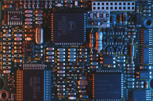
PCBA processing involves connecting various electronic components on a printed circuit board (PCB) through methods such as surface mount technology (SMT), plug-in technology (DIP), and other electronic assembly techniques. The PCBA process flow primarily includes SMT, Automated Optical Inspection (AOI), DIP, Functional Testing (FCT), and additional processes. Due to the size variations of electronic components, different processes and requirements are needed for assembly and insertion. The assembly density of PCBAs is relatively high, and the small size and lightweight nature of electronic products necessitate specific mounting considerations. Additionally, products must meet strict requirements for reliability, seismic resistance, and excellent soldering quality, all of which demand high standards for hardware and software facilities used in PCBA processing.
Currently, numerous testing technologies are employed in electronic assembly testing, including Manual Visual Inspection (MVI), In-Circuit Testing (ICT), Automated Optical Inspection (AOI), Automated X-ray Inspection (AXI), and Functional Testing (FCT). These technologies can be categorized based on whether the PCBA is powered on: electrical testing technologies and non-electrical testing techniques. They can also be classified based on whether the PCBA comes into contact with testing equipment: contact testing methods and non-contact testing technologies.

Manual Inspection During PCBA Assembly
Manual visual inspection involves confirming the mounting, insertion, and soldering of components on the PCBA using human visual comparison. Inspectors typically use their eyes, supplemented with magnifying glasses and microscopes. This method is one of the oldest and most widely used testing techniques.
However, with the advancement of microelectronic surface mount technology (SMT), electronic products are increasingly becoming thinner, lighter, and more compact. The miniaturization of components results in higher density in printed circuit board assemblies (PCBAs). In this context, plug-in components can obstruct each other's visibility, while micro-encapsulated components (like 0201 sizes) and "invisible" solder joints (such as Ball Grid Arrays (BGA), Chip Scale Packages (CSP), and flip-chip assemblies) have become more common in recent years. As a result, the manual visual inspection method of "checking words and colors" no longer reliably ensures the quality of PCBA processing.
In a study, four experienced inspectors evaluated solder joint quality on the same moderately complex circuit board (for instance, a single-layer board with 300 components and 3,500 nodes) four times. The results revealed that the first inspector detected 44% of the defects. The second inspector exhibited only 28% consistency with the first inspector, while the third showed just 12% consistency with the first two, and the fourth inspector had a mere 6% consistency with the first three. This study highlights the subjectivity of manual visual inspection, indicating that it is neither reliable nor economical. Consequently, in current co-processing and manufacturing practice, manual visual inspection is primarily used as a supplementary method.
Why Choose China PCBA Supplier KSPCBA as Your PCBA Assembly Manufacturer?
– Experienced and skilled team
– State-of-the-art equipment
– Strict quality control
– Excellent customer service
– Competitive price

Please send Email to kspcba@c-alley.com or call us through +86 13828766801 Or submit your inquiry by online form. Please fill out below form and attach your manufacturing files( PCB Gerber files and BOM List) if need quotation. We will contact you shortly.
 +86 13828766801
 kspcba@c-alley.com
 https://www.kingshengpcba.com/
 2/F, Building 6, Tangtou 3rd Industrial Zone, Tangtou Community, Shiyan Town, Baoan District, Shenzhen, China, 518108