* On your first PCB Assembly order!
* Up to $300 discount
 C - A L L E Y
 Home | Events | PCB | About Us | News | Contact Us
SEO Keywords Included: PCB baking before SMT, solder paste stencil printing, reflow oven temperature profile, AOI inspection limitations, SMT throw rate optimizatio
1. Why Is PCB Baking Required Before SMT Assembly?
PCB boards tend to absorb moisture during storage and transport. If this moisture isn’t removed before reflow soldering, it can expand rapidly under high temperatures, leading to delamination, popcorning, or even board cracking.
PCB baking helps eliminate this internal moisture. The typical baking conditions are:
Temperature: 120°C ± 5°C
Duration: 2 to 4 hours (depending on board thickness and stack method)
Proper pre-baking prevents thermal damage and improves long-term reliability.
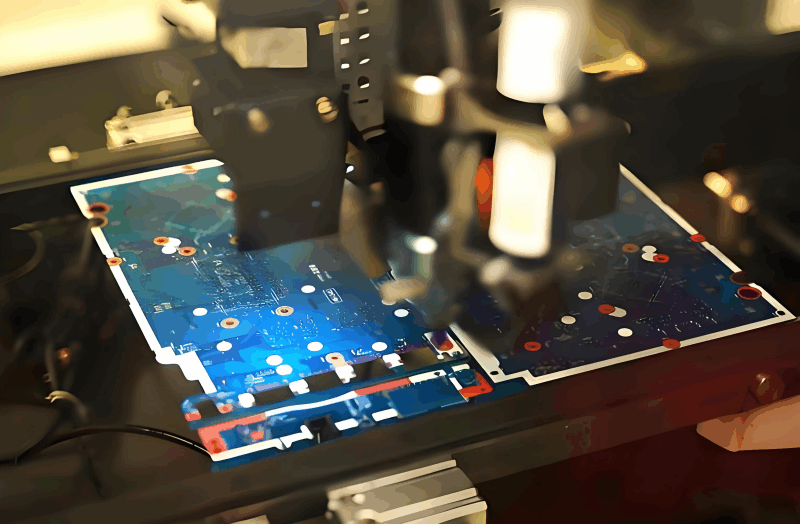
SMT Assembly
2. How to Ensure Uniform Solder Paste Thickness During Stencil Printing?
The uniformity of solder paste application plays a key role in achieving strong and reliable solder joints.
To maintain consistent paste thickness:
Stencil Tension: Should be ≥ 40 N/cm² to prevent sagging
Squeegee Pressure: Adjust within 30–60 N range for proper filling
Printing Speed: Maintain between 10–30 mm/s based on solder paste properties
SPI Monitoring: Use a Solder Paste Inspection (SPI) system to ensure thickness deviation is within ±15μm
Automated monitoring combined with optimized printing parameters helps reduce soldering defects such as bridging or insufficient solder.
3. What’s the Best Practice for Setting the Reflow Soldering Temperature Profile?
A well-designed reflow profile ensures proper solder paste reflow and component integrity. A standard profile includes:
Preheat Zone: Ramp-up rate of 1–3°C/s to 150–180°C
Soak Zone: Hold for 60–120 seconds to activate flux
Reflow Zone: Peak temperature of 220–245°C, dwell time of 40–90 seconds
Cooling Zone: Controlled cool down at ≤ 4°C/s to avoid solder cracks
Adjust the profile based on solder paste specifications and component temperature tolerance for optimal results.
4. Why Does AOI Sometimes Miss Defects Like Cold Solder or Misalignment?
AOI (Automated Optical Inspection) is highly efficient but may still fail to detect certain defects due to:
Component reflectivity and lighting angle
Software algorithm sensitivity
Limitations of 2D inspection in capturing 3D features
To enhance defect detection:
Calibrate AOI parameters regularly
Upgrade to 3D AOI systems, which improve identification of solder volume, height, and bridging with accuracy up to ±10μm
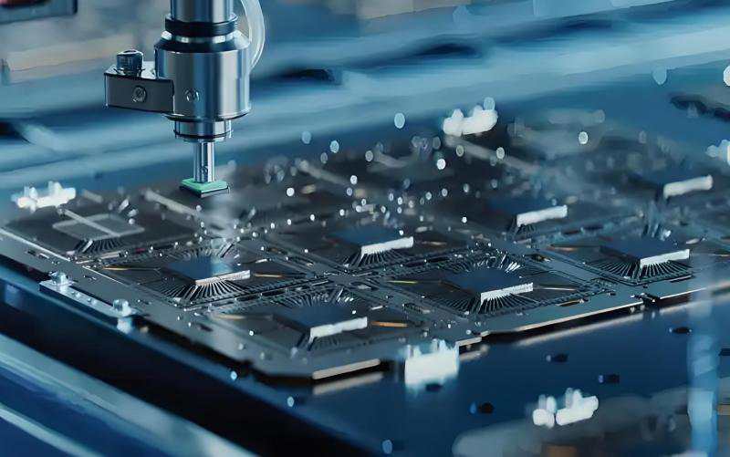
SMT Assembly
5. How to Troubleshoot High Component Throw Rate in Pick-and-Place Machines?
A high throw rate indicates wasted components and reduced production efficiency. Key areas to inspect include:
Nozzle wear and contamination affecting vacuum pickup
Feeder indexing precision and tape alignment
Component data mismatches in the placement library
Improper pickup pressure (optimize to 20–150g) and height (0.1–0.3 mm)
With proper tuning and preventive maintenance, the throw rate can be effectively controlled below 0.3%.
Conclusion
Understanding and optimizing these key SMT processes—from PCB baking and solder paste printing to reflow profiling and AOI tuning—can significantly improve assembly yield and product reliability. For more SMT tips and PCBA insights, follow our blog or contact us for professional one-stop electronics manufacturing solutions.

Please send Email to kspcba@c-alley.com or call us through +86 13828766801 Or submit your inquiry by online form. Please fill out below form and attach your manufacturing files( PCB Gerber files and BOM List) if need quotation. We will contact you shortly.
 +86 13828766801
 kspcba@c-alley.com
 https://www.kingshengpcba.com/
 2/F, Building 6, Tangtou 3rd Industrial Zone, Tangtou Community, Shiyan Town, Baoan District, Shenzhen, China, 518108
We would also like to thank our customers for their trust and support. The company's outstanding achievements are mainly due to the loyalty of our customers, which also encourages and spurs our company to forge ahead.


