* On your first PCB Assembly order!
* Up to $300 discount
 C - A L L E Y
 Home | Events | PCB | About Us | News | Contact Us
Keywords: DFM analysis, PCBA process, PCB assembly, SMT, reflow soldering, Gerber file, BOM, manufacturing defects
In the fast-paced world of electronics manufacturing, new engineers often find themselves overwhelmed by technical jargon and production standards. Terms like "DFM analysis," "stencil aperture design," and "reflow temperature profile" can feel like a foreign language. But in reality, these are the critical elements that determine whether a PCBA project will succeed or fail.
Let’s explore why Design for Manufacturability (DFM) is essential in PCBA manufacturing—and how it can save time, reduce costs, and prevent costly production errors.
What Is PCBA and Why Is DFM So Important?
PCBA (Printed Circuit Board Assembly) is not a single product—it's a dynamic process. It involves mounting electronic components onto a bare PCB and turning them into functional modules through a series of precisely controlled steps. A smartphone motherboard, for example, may go through 20 or more steps before it's fully assembled. At the heart of a successful PCBA project is not only the quality of materials and equipment—but the thoughtfulness of the initial design. That’s where DFM analysis comes in.
What Is DFM Analysis in PCBA?
DFM (Design for Manufacturability) is a set of design guidelines and checks aimed at ensuring a PCB can be manufactured efficiently and reliably. Before a single board is built, engineers use DFM to review:
Pad spacing to ensure stencil printing and soldering can be performed without bridging.
BGA placement to confirm X-ray inspection feasibility.
Thermal layout to avoid hotspots and allow smooth heat dissipation.
A strong DFM review can eliminate up to 80% of potential manufacturing risks before they happen.
From Files to Factory: Where DFM Fits In
???? Gerber Files: The Blueprint of Production
The Gerber file is the bridge between design and manufacturing. It uses RS-274X format to describe every layer of the PCB layout. A well-prepared Gerber ensures your design is interpreted exactly as intended on the production line.
???? BOM (Bill of Materials): The Shopping List of Assembly
The BOM file contains details of every part—from resistors and capacitors to ICs and connectors. Precision matters. An entry like “0805 10kΩ ±1%” tells the purchasing team exactly what to buy, and what substitutions are allowed.
Key PCBA Processes Influenced by DFM
????️ SMT and Stencil Design
In the SMT line, solder paste is applied through a stainless-steel stencil, followed by high-speed component placement and reflow soldering. DFM helps determine correct aperture size, stencil thickness (e.g., 0.13 mm vs. 0.10 mm for BGA), and step-down designs to ensure proper solder volume.
???? Reflow Temperature Curve
The reflow profile is critical. With lead-free solder melting at 217°C, the board must go through multiple thermal zones. DFM ensures the layout can tolerate thermal gradients, and sensitive components are placed away from high-heat areas.
⚙️ DIP and Wave Soldering
Traditional through-hole components like connectors require wave soldering. DFM checks if the pin spacing and layout allow smooth solder flow—avoiding bridges or cold joints.
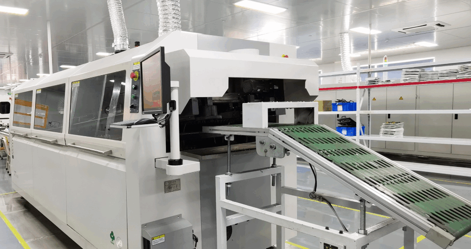
DFM Analysis in PCBA Manufacturing
Testing and Inspection: The Final Gate
???? AOI & X-Ray Inspection
AOI (Automated Optical Inspection) uses cameras to detect misalignment, solder bridges, and missing parts.
X-ray goes deeper—especially for BGA and QFN chips. It verifies hidden solder joints and checks for voids and cracks, often with strict standards like <15% void rate.
⚡ ICT and FCT Testing
ICT (In-Circuit Testing) checks for shorts, opens, and wrong components—within seconds.
FCT (Functional Testing) simulates real working conditions, ensuring every function performs as intended before the board moves to final assembly.
Without proper DFM, these tests may reveal preventable issues that could have been fixed at the design stage.
What Can Go Wrong Without DFM?
Solder bridging due to incorrect pad spacing
Voiding and cold solder joints from poor thermal layout
BGA open circuits due to misaligned stencil design
Inaccessible test points that prevent ICT
X-ray blind spots from poor component placement
These issues lead to rework, delays, higher costs—and in worst cases, total product failure in the field.
Conclusion: DFM Is Not Optional—It's Essential
In PCBA manufacturing, DFM analysis is your first line of defense against failure. By identifying design flaws early, you avoid costly downstream problems and ensure faster, more reliable production.
We offer FREE DFM analysis for all our customers. During the prototyping phase, we also provide pre-production and post-production reports along with expert improvement suggestions—at no extra cost.
Need a trusted PCBA partner with real engineering support? Contact us to start your project with confidence.

Please send Email to kspcba@c-alley.com or call us through +86 13828766801 Or submit your inquiry by online form. Please fill out below form and attach your manufacturing files( PCB Gerber files and BOM List) if need quotation. We will contact you shortly.
 +86 13828766801
 kspcba@c-alley.com
 https://www.kingshengpcba.com/
 2/F, Building 6, Tangtou 3rd Industrial Zone, Tangtou Community, Shiyan Town, Baoan District, Shenzhen, China, 518108
We would also like to thank our customers for their trust and support. The company's outstanding achievements are mainly due to the loyalty of our customers, which also encourages and spurs our company to forge ahead.


