* On your first PCB Assembly order!
* Up to $300 discount
 C - A L L E Y
 Home | Events | PCB | About Us | News | Contact Us
SMT is the core of modern electronic manufacturing, characterized by miniature components, rapid assembly, and dense PCB routing. Once defects occur, not only are rework costs extremely high, but potential risks may also affect the reliability of end product, leading to the Failure of the entire electronic product. Therefore, Inspection throughout the entire process is not "optional" but a lifeline for ensuring Product Quality, controlling costs, and maintaining brand reputation. The following Inspections are crucial:
1.Solder Paste Inspection (SPI)
Statistics show that over 60% of soldering defects originate from this process. SPI utilizes 3D optical scanning to accurately measure the volume, area, height, and offset of the solder paste after printing.
Preventing Subsequent Defects: Excessive solder paste leads to bridging among components (shorts), while insufficient paste results in cold solder joints or opens. By real-time detection and adjustment of printing parameters via SPI (e.g., squeegee pressure, speed, stencil cleaning frequency), the most soldering problems can be completely avoided at the source. Defective boards can be prevented from entering expensive pick-and-place and reflow soldering equipment, which can save significant subsequent repair costs.
Process Control and Optimization: The data chain provided by SPI is fundamental for achieving smart manufacturing and process control, and provides quantitative basis for optimizing the printing process.
2.Post-Component Placement Inspection (Pre-Reflow AOI)
Intercepting Placement Errors: Pick-and-place machines are not 100% perfect; missing components, wrong parts, polarity reversal, misalignment, or even chip cracks may occur. If these issues are discovered at this process, only re-placement or adjustment is required, which incurs the lowest cost.
Avoiding Irreversible Damage: If the boards with above defects flow into the reflow oven, wrong parts and reverse-polarity components may be firmly soldered after high-temperature heating. During repair, there may be a risk of difficult disassembly and damage to surrounding components or PCB pads. Repair costs and time will increase exponentially.
3.Post-Reflow Inspection (Post-Reflow AOI & AXI)
This is the decisive checkpoint for the product's final function and quality. It primarily detects the solder joint status formed after high-temperature reflow soldering.
AOI (Automated Optical Inspection): It primarily inspects visible soldering defects, such as bridging, open circuits, solder balls, component tombstoning, misalignment, and missing components, which is fast and efficient, serving as the primary method for appearance inspection.
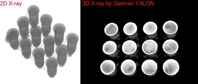
AXI (Automated X-ray Inspection): It is indispensable for inspecting hidden solder joints (e.g., bottom-terminated components such as BGA, CSP, QFN). X-rays can penetrate the component body, clearly revealing the shape, size, and position of solder balls, as well as internal voids. Without AXI, the soldering quality of BGAs is virtually a "blind spot." Once cold solder joints, bridging, or severe voids exist, they can only be detected during subsequent functional testing or even at the client side, by which time the losses will be incalculable.
Summary
The necessity of SMT testing mainly stems from three factors:
Quality Assurance: Ensuring that outgoing products meet stringent reliability standards is the cornerstone for gaining customer trust.
Cost Control: Following the "quality funnel" principle, the earlier defects are detected, the lower the correction cost. SPI and Pre-Reflow AOI are efficient "cost valves."
Process Optimization: The large amount of data generated by inspection equipment provides data-driven decision support for analyzing process shortcomings, optimizing equipment parameters, and improving First Pass Yield (FPY).
Therefore, Kingsheng PCBA regards three inspections as company lifeblood and necessary production process, strictly requiring workers to inspect all boards by standard.

Please send Email to kspcba@c-alley.com or call us through +86 13828766801 Or submit your inquiry by online form. Please fill out below form and attach your manufacturing files( PCB Gerber files and BOM List) if need quotation. We will contact you shortly.
 +86 13828766801
 kspcba@c-alley.com
 https://www.kingshengpcba.com/
 2/F, Building 6, Tangtou 3rd Industrial Zone, Tangtou Community, Shiyan Town, Baoan District, Shenzhen, China, 518108
We would also like to thank our customers for their trust and support. The company's outstanding achievements are mainly due to the loyalty of our customers, which also encourages and spurs our company to forge ahead.


