* On your first PCB Assembly order!
* Up to $300 discount
 C - A L L E Y
 Home | Events | PCB | About Us | News | Contact Us
In the rapidly developing electronics industry, buried and blind via technology has become one of the core processes in high-density interconnect (HDI) printed circuit board (PCB) manufacturing. It significantly enhances the integration and performance of circuit boards by constructing micro conductive channels within multi-layer PCBs that do not penetrate the entire board layer.
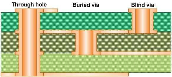
What are Buried and Blind Vias?
Buried and blind vias are a general term for two special types of vias:
1.Blind Via: A via that starts from the PCB surface layer and extends only to a specific depth within an inner layer, without penetrating the entire board layer. It is like a staircase in a tall building, connecting only the top floor and a certain floor in the middle.
2.Buried Via: A via completely hidden within the PCB, connecting two or more inner layers without touching top or bottom layer. It is equivalent to the secret passage that connects the intermediate floors within the building.
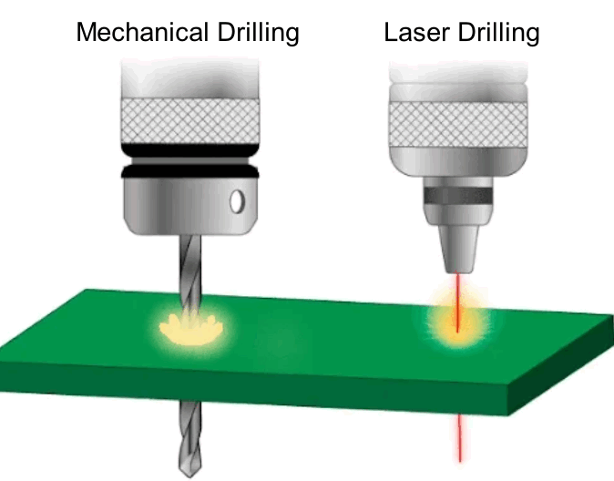
The diameter of these holes is typically smaller than traditional through-hole vias, generally ranging from 0.05 to 0.15 mm. Electrical connection is achieved through laser drilling or mechanical drilling combined with a copper plating process.
What key problems do buried and blind vias address?
1.Increase Routing Density and Save Space
Traditional through-hole vias penetrate all layers, occupying a large amount of board area in the surface. Buried and blind vias allow designers to create vertical connections within the PCB, freeing up surface area for placing more components. This is particularly important in space-constrained products such as smartphones and wearable devices, where internal multi-layer routing avoids all connections being confined to the surface layer.
2.Improve High-Frequency Signal Integrity
Modern high-speed digital circuits and RF systems have extremely high requirements for signal quality. The long columnar structures of traditional through-hole vias will form parasitic capacitance and inductance, leading to signal reflection and distortion. Buried blind vias are shorter, which reduces these parasitic effects, making GHz-level high-frequency signal transmission more stable and reliable.
3.Enhance Power Integrity
By using buried vias in inner layers to construct a distributed power network, the power transmission path can be shortened, impedance and voltage drop can be reduced, and electromagnetic interference (EMI) can be minimized. This provides a cleaner power supply for high-performance processors and ASIC chips.
4.Support Advanced Packaging Technology
Buried and blind via technology is a key technology for achieving high-density packaging such as Chip Scale Package (CSP) and Ball Grid Array (BGA). It enables to create extremely fine interconnect structures on the packaging substrate, meeting the increasing demand for I/O counts in modern chips.
5. Enhance Design Flexibility
Designers can, much like urban planners, construct customized connection schemes between different layers, and no longer be limited by traditional vias that require penetrating all layers. This three-dimensional routing capability greatly expands the possibilities of circuit architecture.
From smartphones to aerospace equipment, buried and blind via technology has become an indispensable cornerstone for the miniaturization and high-performance of electronic products. It is not merely a manufacturing process, but an art for electronic engineers to create infinite possibilities within a limited space—an art that involves the construction of precise channels connecting the future within a microscopic world of square millimeters.

Please send Email to kspcba@c-alley.com or call us through +86 13828766801 Or submit your inquiry by online form. Please fill out below form and attach your manufacturing files( PCB Gerber files and BOM List) if need quotation. We will contact you shortly.
 +86 13828766801
 kspcba@c-alley.com
 https://www.kingshengpcba.com/
 2/F, Building 6, Tangtou 3rd Industrial Zone, Tangtou Community, Shiyan Town, Baoan District, Shenzhen, China, 518108
We would also like to thank our customers for their trust and support. The company's outstanding achievements are mainly due to the loyalty of our customers, which also encourages and spurs our company to forge ahead.


