* On your first PCB Assembly order!
* Up to $300 discount
 C - A L L E Y
 Home | Events | PCB | About Us | News | Contact Us
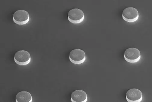
Copper pillar bump technology represents a significant advancement in high-density packaging. Compared to conventional solder bumps, copper pillars maintain shape stability during reflow soldering without collapsing, enabling finer pitch and higher I/O density. Copper pillars also offer superior thermal and electrical conductivity, substantially improving electromigration reliability. However, in PCBA processing, copper pillar bumps impose placement accuracy requirements far more stringent than those of standard SMT processes. The solder cap volume on copper pillars is relatively small, significantly weakening the self-alignment effect during reflow, and minor positional deviations can result in soldering defects.
I. Weakening of the Self-Alignment Effect
In conventional SMT component placement, the solder volume is relatively large. During reflow, molten solder generates surface tension that pulls the component back to the center of the pad. This self-alignment effect compensates for certain placement deviations, providing some tolerance margin for the pick-and-place machine. The solder cap volume of copper pillar bumps is considerably smaller than that of conventional solder balls, and the amount of molten solder generated during reflow is insufficient to produce the surface tension required to pull the copper pillar. The copper pillar itself does not melt during reflow, and its position remains essentially fixed before and after the process. This means that if a placement offset exists prior to reflow, that offset will remain largely unchanged after soldering.
Production data indicates that the placement deviation tolerance for copper pillar bumps on flexible PCBs is significantly lower than for conventional SMT components. Variations in placement position or placement pressure directly affect solder joint quality and final alignment accuracy. For copper pillar bumps with pitches ranging from 20 to 150 μm, any minor placement deviation can lead to bridging or open circuits.
II. Accuracy Requirements for Solder Paste Printing
2.1 Solder Paste Volume Sensitivity
The soldering quality of copper pillar bumps is highly dependent on the consistency of solder paste deposition volume. Excessive solder paste volume can cause the copper pillar to float or tilt during reflow, resulting in coplanarity deviations. Insufficient solder paste volume reduces solder joint strength and may even prevent the formation of an effective connection. In conventional SMT processes, the allowable fluctuation range for solder paste printing is relatively wide. Copper pillar bump processes impose tighter constraints on this tolerance. Stencil design must precisely match the copper pillar diameter and pad dimensions. The aperture size and thickness require accurate calculation to ensure that the solder paste deposition volume remains within a narrow process window. Solder paste selection also needs re-evaluation, with products featuring appropriate powder particle size and rheological properties for fine-pitch printing.
2.2 Impact of Substrate Flatness
Copper pillar bump heights typically range from 30 to 55 μm, with inherent height variations due to the electroplating process. When substrate warpage or localized non-planarity exists, the pressure distribution from the placement head becomes inconsistent. Copper pillars do not undergo compressive deformation during reflow and cannot absorb height differences caused by substrate non-planarity through melting and collapse, as solder bumps can.
In actual production environments, substrate warpage is unavoidable. For conventional SMT processes, warpage can be compensated by increasing solder paste volume or utilizing component self-weight during reflow. The copper pillar bump process lacks such tolerance mechanisms, resulting in significantly higher sensitivity to substrate flatness and placement pressure control.
III. Process Control Strategies for Placement
3.1 Upgraded Pick-and-Place Machine Accuracy Requirements
Copper pillar bump processing demands pick-and-place machines with higher positioning accuracy and repeatability. For copper pillar bump placement, high-precision force and position feedback systems for the placement head are required to ensure consistent placement pressure. The placement head must incorporate closed-loop pressure control functionality to ensure that the impact force on each bump remains within allowable limits, preventing damage to the pad or the copper pillar itself.
3.2 Assembly Method Selection
Three primary assembly methods exist for copper pillar bumps: mass reflow soldering, thermo-compression bonding, and Au-Cu thermo-compression bonding. Mass reflow soldering is suitable for high-volume, low-cost production but imposes the most stringent placement accuracy requirements, as this process lacks compensation mechanisms. Thermo-compression bonding can compensate for placement deviations to a certain extent through applied pressure and heat, albeit at lower production efficiency. For ultra-fine pitch applications below 60 μm, thermo-compression bonding is typically required.
3.3 Enhanced AOI Inspection
After copper pillar bump soldering, automated optical inspection (AOI) coverage and inspection criteria must be strengthened. Key inspection focus areas include copper pillar positional offset, solder wetting morphology, and bridging defects. Due to the dense arrangement of copper pillar bumps, the inspection system must possess high resolution capable of identifying minor positional deviations and solder anomalies. X-ray inspection is also a necessary method in certain cases to examine voiding conditions within the solder.
Conclusion
The challenge that copper pillar bump soldering presents to placement accuracy fundamentally stems from the way its structural characteristics compress the process tolerance window. From solder paste printing to component placement and reflow soldering, the error control requirements at each stage exceed those of conventional SMT processes. For PCBA manufacturers undertaking copper pillar bump products, a comprehensive assessment of existing equipment capability, optimized stencil design and process parameters, and stricter inspection standards are essential. Only by embedding placement accuracy control throughout the entire production process can manufacturers fully leverage the technical advantages of copper pillar bump technology in high-density packaging while maintaining acceptable yield rates.

Please send Email to kspcba@c-alley.com or call us through +86 13828766801 Or submit your inquiry by online form. Please fill out below form and attach your manufacturing files( PCB Gerber files and BOM List) if need quotation. We will contact you shortly.
 +86 13828766801
 kspcba@c-alley.com
 https://www.kingshengpcba.com/
 2/F, Building 6, Tangtou 3rd Industrial Zone, Tangtou Community, Shiyan Town, Baoan District, Shenzhen, China, 518108
We would also like to thank our customers for their trust and support. The company's outstanding achievements are mainly due to the loyalty of our customers, which also encourages and spurs our company to forge ahead.


