* On your first PCB Assembly order!
* Up to $300 discount
 C - A L L E Y
 Home | Events | PCB | About Us | News | Contact Us
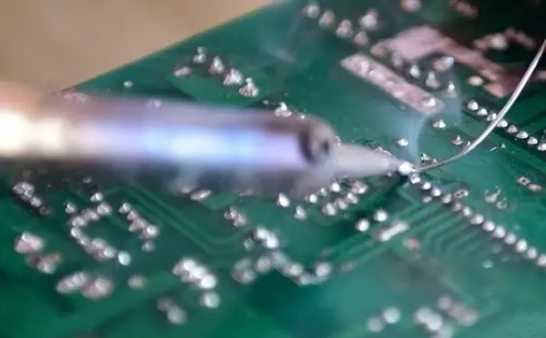
Since the EU RoHS Directive officially took effect in 2006, the electronics manufacturing industry has fully transitioned to lead-free soldering processes. Lead-free solder alloys (such as SAC305) have melting points approximately 30°C to 40°C higher than traditional tin-lead solders, raising reflow soldering peak temperatures from the previous 220°C–230°C range to 245°C–260°C. This upward shift in the temperature window has directly altered the thermal stress environment that printed circuit boards endure during PCBA processing. In actual production, issues such as blistering, delamination, barrel cracking, and reduced solder joint reliability caused by improper substrate selection have increased year over year. For PCBA contract manufacturers, selecting high glass transition temperature (TG) laminates under lead-free soldering conditions has evolved from a technical recommendation to a mandatory requirement for quality control.
I. Core Performance Parameters of High-TG Laminates
1.1 Definition and Classification of Glass Transition Temperature (TG)
Glass transition temperature is the critical point at which the resin transitions from a rigid glassy state to a soft rubbery state. Standard FR-4 laminates exhibit TG values in the range of 130°C–140°C, mid-TG materials fall between 150°C–160°C, and high-TG laminates are defined as having TG ≥ 170°C, with certain specialty materials reaching above 200°C. This parameter directly determines the dimensional stability and mechanical strength retention of the substrate at elevated temperatures.
1.2 Thermal Decomposition Temperature (TD) and Z-Axis Coefficient of Thermal Expansion
Beyond TG value, high-TG laminates typically exhibit higher thermal decomposition temperatures (TD > 340°C) and lower Z-axis coefficients of thermal expansion (CTE, typically below 50 ppm/°C). At lead-free soldering peak temperatures, lower CTE means better expansion matching between the plated copper in vias and the resin matrix, thereby reducing tensile stress on the barrel walls.
II. Three Major Challenges of Lead-Free Soldering Processes to Laminates
2.1 Higher Peak Temperatures Induce Resin Softening Risks
In lead-free reflow profiles, PCB surface temperatures remain above 245°C for 40 to 90 seconds. If standard TG laminates (TG ≤ 140°C) are used, the resin has already fully entered the rubbery state at these temperatures, with the elastic modulus dropping by more than 60%. Under these conditions, the board is highly susceptible to irreversible warpage during clamping or cooling phases, resulting in bridging or head-in-pillow defects on fine-pitch components such as BGAs.
2.2 Thermal Accumulation Effects of Multiple Reflow Cycles
Double-sided assembly and complex mixed-technology boards require 2 to 3 reflow cycles. Each heating cycle further degrades the cross-linked resin structure of standard laminates, with cumulative thermal stress generating sustained tensile forces in the Z-axis direction. Experimental data shows that after two lead-free reflow cycles, the interlaminar bond strength of standard FR-4 decreases by approximately 35%, whereas the reduction for high-TG laminates remains within 12%.
2.3 Coupled Effects of Thermal Stress and Moisture
PCBs absorb ambient moisture during storage and processing. During lead-free soldering, moisture rapidly vaporizes at high temperatures, with volumetric expansion generating internal vapor pressure. Low-TG laminates exhibit insufficient peel strength at elevated temperatures, making them prone to blistering (delamination) beneath pads or over large copper areas. High-TG laminates, due to their higher cross-linking density and lower moisture permeability, effectively reduce the probability of delamination failures.
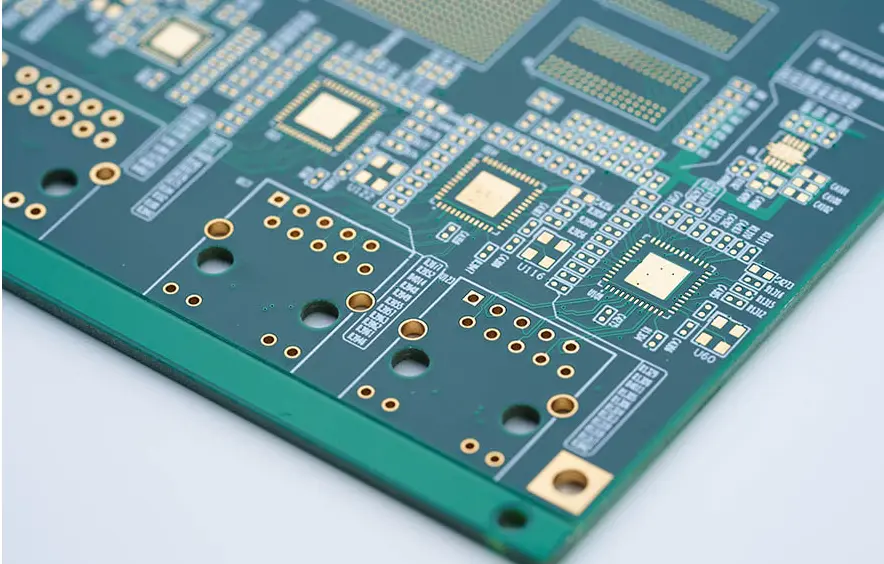
III. Direct Processing Benefits of High-TG Laminates
3.1 Reduction in Soldering Defect Rates
After adopting laminates with TG ≥ 170°C, PCBA factories can reduce warpage-related defect rates from 2.3%–3.5% (observed with conventional laminates) to below 0.5% in lead-free processes. For thin boards with thickness below 1.6mm in particular, dimensional stability improves significantly, and placement alignment accuracy (X/Y offset) can be controlled within ±50μm. 3.2 Improved Electrical Reliability
High-TG materials maintain higher volume resistivity and breakdown voltage withstand capability at elevated temperatures. In solder insulation resistance (SIR) tests conducted after lead-free soldering, the failure threshold of high-TG laminates is 1 to 2 orders of magnitude higher than that of standard laminates, which is particularly critical for high-density routing and impedance-controlled RF boards.
3.3 Extended Product Service Life
Thermal cycling test results (-40°C to 125°C, 1000 cycles) indicate that solder joint fatigue life is extended by approximately 40% with high-TG laminates. This improvement primarily stems from their lower Z-axis expansion, which reduces reciprocating tensile stress on plated through-hole copper walls, thereby delaying crack initiation.
IV. Selection Misconceptions and Cost Trade-Offs
4.1 Common Misconception: TG Value as the Sole Criterion
Some procurement departments blindly pursue high TG values while overlooking the resin system (such as DICY-cured vs. phenolic-cured), reinforcement materials (open-weave vs. flat-weave glass fabrics), and filler types. In actual selection, a comprehensive assessment should incorporate three heat-resistance metrics: TD (recommended ≥ 340°C), T260 (time to delamination at 260°C, recommended ≥ 30 minutes), and T288 (heat resistance time at 288°C, recommended ≥ 5 minutes).
4.2 Cost-Benefit Analysis: Material Premium vs. Failure Costs
High-TG laminates are priced 20% to 35% higher than standard FR-4. However, for a factory producing 100,000 double-sided boards annually, using standard laminates results in comprehensive losses from blistering, warpage, and reliability-related returns amounting to approximately 4.5%–6% of total output value. After switching to high-TG laminates, these losses can be compressed to below 1.2%. The net savings comfortably offset the material premium, leaving a clear surplus.
Conclusion
The rigid temperature requirements of lead-free soldering processes mandate that PCBA contract manufacturers designate TG value as a critical material selection parameter. High-TG laminates directly address the pain points of lead-free processing—warpage, delamination, and barrel cracking—through higher glass transition temperatures, lower Z-axis coefficients of thermal expansion, and superior thermal decomposition resistance. For volume production orders, it is recommended to adopt TG ≥ 170°C, TD ≥ 340°C, and T260 ≥ 30 minutes as the minimum qualification criteria, while also performing targeted validation based on specific layer counts, board thicknesses, and component types. Given the irreversible industry trend toward lead-free assembly, high-TG laminates are no longer a value-added option but a fundamental threshold for ensuring soldering yield and long-term reliability. PCBA factories should translate this understanding into internal material selection specifications and embed it into quotation review and design-for-manufacturing (DFM) screening workflows, thereby reducing total life-cycle quality risks.

Please send Email to kspcba@c-alley.com or call us through +86 13828766801 Or submit your inquiry by online form. Please fill out below form and attach your manufacturing files( PCB Gerber files and BOM List) if need quotation. We will contact you shortly.
 +86 13828766801
 kspcba@c-alley.com
 https://www.kingshengpcba.com/
 2/F, Building 6, Tangtou 3rd Industrial Zone, Tangtou Community, Shiyan Town, Baoan District, Shenzhen, China, 518108
We would also like to thank our customers for their trust and support. The company's outstanding achievements are mainly due to the loyalty of our customers, which also encourages and spurs our company to forge ahead.


