* On your first PCB Assembly order!
* Up to $300 discount
 C - A L L E Y
 Home | Events | PCB | About Us | News | Contact Us
As electronic devices trend toward smaller size and higher performance, BGA packaging is widely used because of its high pin density, excellent electrical conductivity, and heat dissipation properties. In PCBA processing, BGA fan-out refers to the routing from BGA pads to outer layers. A proper fan-out strategy directly affects the balance between routing density and manufacturability. Overly dense fan-out may cause short circuits, pad peeling, or difficult rework; overly loose fan-out wastes PCB space, increases layer count, and raises costs. This article provides actionable solutions for balancing design, process, and inspection.
1. Setting Core Parameters for BGA Fan-out
1.1 Pad Size and Solder Mask Definition
BGA pad diameter is typically 80% of the ball diameter. Non-solder-mask defined (NSMD) pads are recommended, meaning the solder mask opening is larger than the pad, preventing mask intrusion onto the pad area. For 0.4mm pitch BGA, pad diameter should be 0.2mm-0.25mm, with a solder mask opening of 0.28mm-0.33mm, leaving a fan-out channel width of no less than 0.1mm.
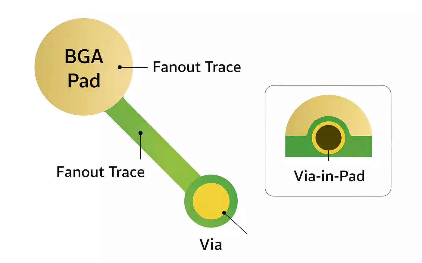
1.2 Via Type and Size
Use via-in-pad or vias between pads. For pin pitches below 0.5mm, via-in-pad requires copper electroplating and filling.
For vias between pads, laser micro-vias are recommended, with a hole diameter of 0.075mm-0.1mm and an annular ring of 0.025mm. For standard 0.8mm pitch BGA, mechanical vias can be used, with a hole diameter of 0.2mm, annular ring of 0.05mm, and a via-to-pad spacing of at least 0.075mm.
1.3 Minimum Trace Width and Spacing
Set based on PCB manufacturer capabilities. For volume production, 0.09mm trace width and 0.09mm spacing are recommended. For high-density designs, this can be reduced to 0.075mm/0.075mm, but factory yield data must be verified.
2. Layer-by-Layer Fan-out Strategy by Pin Region
2.1 Outer Layer Fan-out: Peripheral Pins
The outermost two rows of pins are routed directly on the outer layer. The first row uses short, straight traces at 0 or 45 degrees, with trace length not exceeding 2mm. The second row uses vias to transition to inner layers, placing vias diagonally adjacent to the pins. The outer layer copper pour should be continuous, and no isolated copper pieces should appear.
2.2 Inner Layer Fan-out: Core Area
Inner pins must be routed via vias to inner layers. Use a "grid" fan-out pattern: place one via at the center of every four pads, connecting to all four pads. This structure allows 25%-30% of pins to be fanned out per layer. Assign remaining pins to a second inner layer, staggering via locations.
2.3 Power and Ground Pin Handling
Fan out power and ground pins directly to inner-layer power/ground planes, without occupying signal routing channels. Adjacent power pins share vias to reduce via count. Place at least one decoupling capacitor connection via for every 4-6 power/ground pins in each BGA region.
3. Design for Manufacturability (DFM) Checklist
3.1 Solder Mask Bridge Retention
Maintain a solder mask bridge width of at least 0.05mm between adjacent pads. If pad-to-pad spacing is less than 0.1mm, consider reducing pad size or using solder-mask-defined (SMD) pads.
3.2 Via-to-Pad Clearance
The distance from via edge to pad edge should be at least 0.05mm. Smaller clearances can cause shorts during solder paste printing or flux wicking into vias. DFM software can automatically check this parameter.
3.3 Thermal Balance Design
Add 1-2 thermal relief pads (with opening width 0.2mm-0.25mm) near power and ground vias to prevent excessive heat dissipation during reflow, which could cause cold solder joints. Do not use thermal relief for signal vias; maintain full copper connection.
3.4 Reworkability Margin
Reserve at least 1.5mm of via-free area around the BGA periphery for hot air rework heating and pry tool placement. Avoid stacking vias densely in the interior, as this creates localized high thermal mass during rework.
4. Verification Methods
4.1 Impedance and Loss Testing
After fan-out, differential impedance should be controlled within 100Ω ±10%, single-ended within 50Ω ±10%. Use TDR testing at fan-out vias. When the deviation exceeds 15%, the size of the via antipad needs to be adjusted.
4.2 X-ray Inspection
After first-article BGA assembly, use 2D X-ray to inspect the alignment between fan-out vias and BGA solder balls. Misalignment between solder balls and vias should not exceed 0.05mm. If unfilled vias are found under solder balls, classify as a design defect.
4.3 Cross-section Analysis
Randomly select 1-2 samples per batch for metallographic cross-sectioning. Check that copper plating fill height in via-in-pad is flush with the pad surface. Any depression or protrusion exceeding 0.02mm requires adjustment of the plating process or supplier change.
Conclusion
The essence of BGA fan-out is making quantitative trade-offs between signal integrity and production yield. Running a BGA-specific design rule check using DFM software before each prototype submission can eliminate more than 80% of fan-out-related defects.

Please send Email to kspcba@c-alley.com or call us through +86 13828766801 Or submit your inquiry by online form. Please fill out below form and attach your manufacturing files( PCB Gerber files and BOM List) if need quotation. We will contact you shortly.
 +86 13828766801
 kspcba@c-alley.com
 https://www.kingshengpcba.com/
 2/F, Building 6, Tangtou 3rd Industrial Zone, Tangtou Community, Shiyan Town, Baoan District, Shenzhen, China, 518108
We would also like to thank our customers for their trust and support. The company's outstanding achievements are mainly due to the loyalty of our customers, which also encourages and spurs our company to forge ahead.


