* On your first PCB Assembly order!
* Up to $300 discount
 C - A L L E Y
 Home | Events | PCB | About Us | News | Contact Us
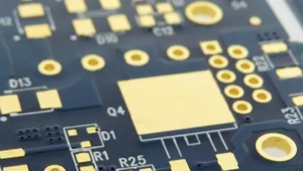
In the PCBA manufacturing process, the choice of PCB surface finish directly affects soldering quality and long-term reliability. The Electroless Nickel Immersion Gold (ENIG) process is widely used for high-density, high-reliability circuit boards due to its good flatness, solderability, and oxidation resistance. However, when the thickness of the PCB gold plating exceeds process specifications, a soldering defect known as "gold embrittlement" can occur. Gold embrittlement manifests as the formation of brittle gold-tin intermetallic compounds within the solder joint, leading to degraded mechanical properties of the joint and a tendency to fracture under mechanical stress or thermal cycling conditions. This article analyzes the formation mechanism of gold embrittlement, examines the specific effects of excessive gold plating thickness on the soldering process, and proposes corresponding control and inspection methods.
1. Formation Mechanism of Gold Embrittlement
1.1 Reaction Path of Gold in the Solder Joint
During the reflow soldering process, the gold layer on the PCB surface quickly dissolves into the molten solder. Gold reacts with tin to form intermetallic compounds such as AuSn₄. When the gold content in the solder joint exceeds 3% to 5% by weight, these compounds precipitate in acicular or plate-like morphologies, distributed within the solder matrix or at the interface. 1.2 Structural Characteristics of the Brittle Phase
The AuSn₄ compound is hard and brittle, with a fracture elongation of less than 1%. Under mechanical stress, this compound cannot absorb energy through plastic deformation and instead becomes a preferential path for crack initiation and propagation. Numerous failure analysis cases related to gold embrittlement show fracture surfaces exhibiting typical intergranular brittle fracture morphology.
2. Causes of Excessive Gold Plating Thickness and Risk Thresholds
2.1 Process Control Failures
According to IPC-4552 standard, the recommended gold thickness for the ENIG process is between 0.05 µm and 0.10 µm. Some PCB manufacturers increase the gold thickness to above 0.15 µm to improve storage oxidation resistance or meet appearance requirements. When the gold thickness exceeds 0.20 µm, the risk of gold embrittlement increases significantly.
2.2 Critical Point of Gold Content
Using a standard gold thickness of 0.05 µm, the corresponding gold weight fraction in the solder joint is approximately 0.5%. When the gold thickness reaches 0.15 µm, the gold content in the solder joint rises to about 1.5%, still within a controllable range. At a thickness of 0.30 µm, the gold content approaches the critical value of 3%. When the thickness exceeds 0.50 µm, the gold content in the solder joint generally surpasses 5%, at which point the probability of brittle fracture increases significantly.
3. Specific Effects of Gold Embrittlement on Soldering Reliability
3.1 Degraded Mechanical Shock Resistance
Under drop or vibration conditions, the ability of a gold-embrittled solder joint to absorb impact energy is significantly reduced. Comparative test data shows that a solder joint with a gold thickness of 0.05 µm can withstand more than 15 impacts in a 60-inch drop test without failure. A solder joint with a gold thickness of 0.30 µm experiences an average failure count reduced to 3 to 5 impacts under the same test conditions.
3.2 Shortened Thermal Cycle Life
During thermal cycling, the difference in coefficient of thermal expansion between different materials generates cyclic shear stress. A gold-embrittled solder joint, lacking sufficient plastic deformation capability, rapidly propagates cracks along the AuSn₄ phase interface. In a practical case, a communication module exhibited a reduction in thermal cycle life for its BGA package from the required 1000 cycles down to 200 cycles, due to a PCB gold thickness of 0.45 µm.
3.3 Pad Peeling During Rework
During manual soldering or rework operations, a gold-embrittled solder joint, subjected to localized high temperatures and external force, is prone to separation between the solder pad and the nickel layer. This manifests as a fracture at the interface between the gold layer and the nickel layer, leaving a complete circular pad mark while the component lead has detached.
4. Methods for Detecting and Judging Gold Embrittlement
4.1 Gold Thickness Measurement
Use X-ray fluorescence spectrometry to inspect the gold thickness of incoming PCBs. For each batch, randomly sample at least five boards, and measure no fewer than three locations per board. Batches with a gold thickness exceeding 0.15 µm are classified as high-risk and require confirmation with the customer regarding acceptance.
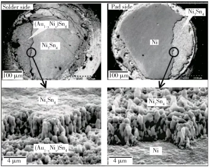
4.2 Cross-Sectional Microanalysis of Solder Joints
For suspected gold-embrittled solder joints, perform cutting, grinding, and polishing. Use a scanning electron microscope to observe the morphology of intermetallic compounds within the solder joint. If a continuous acicular AuSn₄ layer or an accumulation of plate-like compounds is observed, and the gold element mapping shows a network-like distribution, a failure due to gold embrittlement can be determined.
5. Prevention and Control Measures for Gold Embrittlement
5.1 Incoming Material Control
Specify in procurement documents that the gold thickness must be between 0.05 µm and 0.10 µm. Perform thickness spot checks on each incoming batch. Reject non-conforming batches directly.
5.2 Process Optimization
For situations where PCBs with excessively thick gold plating must be used, a secondary gold removal process can be applied. Print solder paste on the pads and perform a reflow pass to dissolve the gold layer into the solder, then use solder wick to remove the gold-containing solder. This operation increases process cost but effectively reduces the gold content in the solder joint to a safe range.
5.3 Design Alternatives
For high-reliability products, recommend using Electroless Nickel Electroless Palladium Immersion Gold (ENEPIG) or direct Nickel-Palladium-Gold finish. The palladium layer blocks excessive dissolution of gold into the solder, reducing the risk of gold embrittlement by over 80%.
Conclusion
The essence of the gold embrittlement phenomenon is that when the gold plating thickness exceeds the process window, an excessive amount of gold in the solder joint leads to the accumulation of brittle intermetallic compounds.

Please send Email to kspcba@c-alley.com or call us through +86 13828766801 Or submit your inquiry by online form. Please fill out below form and attach your manufacturing files( PCB Gerber files and BOM List) if need quotation. We will contact you shortly.
 +86 13828766801
 kspcba@c-alley.com
 https://www.kingshengpcba.com/
 2/F, Building 6, Tangtou 3rd Industrial Zone, Tangtou Community, Shiyan Town, Baoan District, Shenzhen, China, 518108
We would also like to thank our customers for their trust and support. The company's outstanding achievements are mainly due to the loyalty of our customers, which also encourages and spurs our company to forge ahead.


