* On your first PCB Assembly order!
* Up to $300 discount
 C - A L L E Y
 Home | Events | PCB | About Us | News | Contact Us
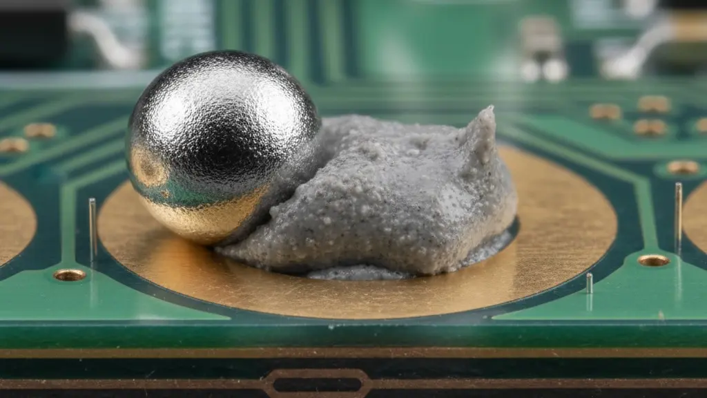
The head-in-pillow defect is a common soldering quality issue in PCBA processing. It manifests as an incomplete connection between the component lead and the solder, where the lead appears to contact the solder joint but a microscopic gap remains. This defect is particularly prevalent in packages such as BGA and QFN. The high cost of rework and difficulty of detection are the primary challenges of head-in-pillow defects. As a PCBA contract manufacturer, controlling the defect at the design source is more effective than relying solely on process adjustments. Pad design directly affects the thermal response and wetting behavior of the solder joint interface and is a key factor in reducing the occurrence of head-in-pillow defects.
1. Mechanism of Head-in-Pillow Defects and the Role of Pad Design
The root cause of a head-in-pillow defect is the failure to form an intermetallic compound between the component lead and the solder. During reflow, the solder on the pad reaches its melting point and fully wets the pad before the component lead. Due to oxidation or thermal lag on the lead side, the solder fails to climb up the lead. When the solder enters the solidification stage and the lead begins to wet, an oxide film has already formed on the solder surface, resulting in a false contact.
Pad design influences this mechanism in three ways. First, pad size determines the solder volume; insufficient solder cannot fill the gap between the lead and the pad. Second, pad shape affects the solder spreading direction; an improper shape causes solder to preferentially flow to one side. Third, pad surface finish affects wetting time, as different finishes have different wetting onset temperatures.
2. Pad Dimension Design Methods to Reduce Head-in-Pillow Defects
2.1 Controlling the Ratio of Pad Width to Lead Width
For BGA components, the PCB pad diameter should be 80% to 85% of the solder ball diameter. For a solder ball diameter of 0.3mm, the pad diameter should be 0.24 to 0.255mm. This ratio ensures that the molten solder ball has sufficient volume to fill the vertical space between the pad and the component body. An excessively large pad causes solder to spread outward, leaving the vertical gap between the pad and the lead unfilled and increasing the risk of head-in-pillow.
For QFN components, the thermal pad width should be inset 0.05 to 0.10mm per side relative to the component's exposed pad. Signal pad width should match the lead width, with length extending 0.2mm beyond the lead outline.
2.2 Effect of Pad Length on Vertical Solder Stack Height
Pad length determines the horizontal spreading distance of the solder. When the pad is too long, solder preferentially flows along the length direction, reducing vertical stack height and diminishing the contact opportunity between the lead and the solder. The recommended pad length is 1.2 to 1.5 times the lead length. If the pad length exceeds this range, compensation must be made through stencil aperture design, reducing the aperture length to limit horizontal spreading.
3. Optimization Strategies for Pad Shape and Surface Finish
3.1 Asymmetric Pad Design to Control Molten Solder Flow
Head-in-pillow defects occur more frequently at the edges of components. The reason is the thermal mass asymmetry on both sides of the edge pads, causing the solder on one side to melt and flow away first. An asymmetric pad design can mitigate this issue. The specific method is to add a blocking structure at the outer edge of the pad, such as a solder mask defined line at the pad end. This structure retains the solder in the central pad area, maintaining the vertical contact height between the lead and the solder.
3.2 Precise Definition of Solder Mask Openings
The solder mask opening should not be larger than the actual pad size. An excessively large opening allows solder to spread to non-pad areas, reducing the effective soldering volume. The recommended opening size is equal to the pad size, with a tolerance within 0.05mm. When the solder mask bridge width is less than 0.1mm, consider removing the bridge and using a single large opening, but add solder mask defined lines between adjacent pads.
3.3 Recommendations for Selecting Surface Finish
The wetting characteristics of different surface finishes directly impact head-in-pillow defects. ENIG provides a stable wetting surface with a low wetting onset temperature; solder spreads quickly after melting. OSP has a narrower wetting window. The initial wetting speed is slower during the early melting phase. When dwell time in the high-temperature zone is insufficient, head-in-pillow defects become more likely. For products sensitive to head-in-pillow defects, ENIG or electrolytic Ni/Au finishes are preferred. If OSP must be used, extend the time above liquidus during reflow to 60 to 90 seconds accordingly.
Conclusion
Eliminating head-in-pillow defects cannot rely solely on process parameter adjustments. The proportional control of pad dimensions, blocking design using asymmetric shapes, precision management of solder mask openings, and proper selection of surface finishes together form a systematic approach to preventing head-in-pillow defects from the design side.

Please send Email to kspcba@c-alley.com or call us through +86 13828766801 Or submit your inquiry by online form. Please fill out below form and attach your manufacturing files( PCB Gerber files and BOM List) if need quotation. We will contact you shortly.
 +86 13828766801
 kspcba@c-alley.com
 https://www.kingshengpcba.com/
 2/F, Building 6, Tangtou 3rd Industrial Zone, Tangtou Community, Shiyan Town, Baoan District, Shenzhen, China, 518108
We would also like to thank our customers for their trust and support. The company's outstanding achievements are mainly due to the loyalty of our customers, which also encourages and spurs our company to forge ahead.


