* On your first PCB Assembly order!
* Up to $300 discount
 C - A L L E Y
 Home | Events | PCB | About Us | News | Contact Us
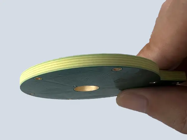
In PCBA manufacturing, high-thickness copper boards generally refer to circuit boards with a finished copper weight of 3 oz+. These boards are commonly found in high-current power modules, automotive electronics, industrial control equipment, and other applications with strict requirements for heat dissipation and current-carrying capacity. Compared to standard 1oz or 2oz copper boards, the copper layer volume and thermal mass of 3oz+ boards increase significantly, and the difference in coefficient of thermal expansion between copper and the FR4 substrate becomes more pronounced. Improper preheating or reflow parameters can easily lead to issues such as inner-layer copper delamination, barrel cracks, pad lifting, or insufficient solder joint formation. Based on production data, this article provides a set of preheating and reflow strategies specifically for high-thickness copper boards.
1. Thermal Characteristics of High-Thickness Copper Boards and Their Challenges to Soldering
A 3oz copper layer is approximately 105 microns thick, while 4oz reaches 140 microns. Copper has a thermal conductivity of about 385 W/(m·K), whereas FR4 is only 0.3–0.4 W/(m·K). Solder heat dissipates rapidly and laterally through the copper layer, causing the following problems:
Therefore, the goal of preheating is not simply to raise temperature, but to achieve thermal equilibrium across the entire board.
2. Preheating Strategy: Ramped Heating and Soaking
2.1 Three-Stage Preheating Profile
For 3oz and above copper boards, the preheating zone should be divided into three independent stages:
Stage 1: Low ramp rate (1.0–1.5°C/sec)
Raise the temperature from room temperature to 110°C. The slow ramp allows the copper and substrate to expand together, reducing internal stress. This stage accounts for 40% of the total preheating zone length.
Stage 2: Soaking plateau (hold at 110°C for 60–90 seconds)
110°C is the activation starting point for most no-clean solder paste solvents. The plateau allows temperatures in high-copper areas to catch up to low-copper areas, keeping the temperature difference across the board within ±5°C. Practical verification should be done using thermocouples placed at the board edge and center.
Stage 3: Fast ramp to activation temperature (2.0°C/sec)
Ramp from 110°C to 150–160°C, entering the solder paste activation window.
2.2 Preheating Exit Criteria
Time should not be the sole criterion. The minimum temperature at the coldest point on the board must reach 150°C. For 3oz boards, the maximum temperature difference across the board at the preheating exit should not exceed 8°C. For 4oz boards, this tolerance may be extended to 10°C. If the difference exceeds these limits, extend the soaking time or reduce the conveyor speed.
3. Reflow Strategy: Zone Compensation and Peak Adjustment
3.1 Temperature Offset Settings per Zone
Based on standard reflow parameters for 1oz boards, apply the following offsets for high-thickness copper boards:
For SAC305 solder paste (melting point 217°C), the measured peak temperature for a 3oz board should reach 240–245°C, compared to 235–240°C for standard boards. The reason for these higher setpoints is the heat absorption and lateral conduction of the copper layer.
3.2 Reflow Time Adjustments
Extending TAL ensures sufficient time for the solder to flow in high-copper areas, preventing insufficient wetting due to local incomplete melting. However, do not exceed the maximum limit specified by the solder paste manufacturer.
3.3 Cooling Rate Control
High-thickness copper boards retain significant heat after reflow. The recommended cooling rate is 3–4°C/sec using forced air. Slow cooling (<2°C/sec) can cause differential shrinkage between the copper and substrate during the cooling phase, leading to delamination. Excessive cooling (>5°C/sec) may cause board warpage or microcracks in ceramic capacitors.
4. Three Verification Methods in Production
First, use a temperature profiling board made from the same batch of high-thickness copper boards. Thermocouples should be placed at the following locations: center of large copper area, non-copper area, large component pad, and board edge.
Second, for the first article of each batch, use X-ray inspection to check the connection between inner-layer copper and barrel wall.
Third, perform cross-section analysis on soldered high-thickness boards, focusing on the interface between the barrel wall and inner-layer copper rings for any voids.
Conclusion
Preheating and reflow for high-thickness copper boards are fundamentally thermal management challenges. The core approach is to eliminate initial temperature differences through staged preheating, then compensate for the copper layer's heat dissipation effect by elevating reflow temperatures, and finally release thermal stress through controlled cooling.

Please send Email to kspcba@c-alley.com or call us through +86 13828766801 Or submit your inquiry by online form. Please fill out below form and attach your manufacturing files( PCB Gerber files and BOM List) if need quotation. We will contact you shortly.
 +86 13828766801
 kspcba@c-alley.com
 https://www.kingshengpcba.com/
 2/F, Building 6, Tangtou 3rd Industrial Zone, Tangtou Community, Shiyan Town, Baoan District, Shenzhen, China, 518108
We would also like to thank our customers for their trust and support. The company's outstanding achievements are mainly due to the loyalty of our customers, which also encourages and spurs our company to forge ahead.


