* On your first PCB Assembly order!
* Up to $300 discount
 C - A L L E Y
 Home | Events | PCB | About Us | News | Contact Us
I. Routing Overview
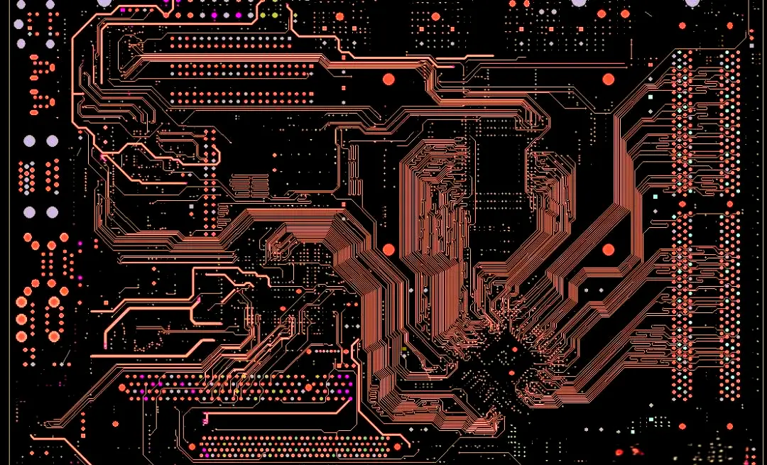
Routing is the most critical, detailed, and labor-intensive step in PCB design. It includes single-sided, double-sided, and multi-layer routing. Two methods exist: automatic and interactive. Before auto-routing, pre-route critical nets manually. Avoid parallel input/output traces to prevent reflection; add ground isolation if necessary. Adjacent layers should route perpendicularly to reduce parasitic coupling.
Auto-routing success depends on good placement. Set rules for via count, bend limits, and step size. Use exploratory routing for short nets, then maze routing for global path optimization, allowing re-routing to improve results.
For high-density designs, blind and buried vias save routing channels compared to through-holes.
II. Power & Ground Handling
Poor power/ground design degrades performance. Key measures:
III. Mixed-Signal Grounding
Separate digital and analog grounds internally; connect them at a single point near the PCB interface (e.g., connector). Do not merge them inside the board.
IV. Routing on Power/Ground Layers
If signal layers are insufficient, route on power or ground layers—preferably on the power layer to preserve ground plane integrity.
V. Thermal Relief for Large Copper Areas
Use thermal relief pads (cross-shaped) for component leads connected to large copper areas to prevent soldering defects caused by excessive heat dissipation.
VI. Routing Grid System
Set grid based on standard 0.1-inch (2.54 mm) pitch or its integer multiples (e.g., 0.05", 0.025"). A balanced grid density ensures routability without excessive data load.
VII. Design Rule Check (DRC)
Verify:
VIII. Netlist Verification
Always verify netlist consistency between schematic and PCB before fabrication.
IX. Simulation
Perform simulation (especially for high-frequency digital circuits) to reduce debugging time.
X. Frequently Asked Questions (FAQs)
A. Software & Setup

Please send Email to kspcba@c-alley.com or call us through +86 13828766801 Or submit your inquiry by online form. Please fill out below form and attach your manufacturing files( PCB Gerber files and BOM List) if need quotation. We will contact you shortly.
 +86 13828766801
 kspcba@c-alley.com
 https://www.kingshengpcba.com/
 2/F, Building 6, Tangtou 3rd Industrial Zone, Tangtou Community, Shiyan Town, Baoan District, Shenzhen, China, 518108
We would also like to thank our customers for their trust and support. The company's outstanding achievements are mainly due to the loyalty of our customers, which also encourages and spurs our company to forge ahead.