* On your first PCB Assembly order!
* Up to $300 discount
 C - A L L E Y
 Home | Events | PCB | About Us | News | Contact Us
In PCB reverse engineering, schematic extraction refers to deriving the circuit diagram from PCB layout files or directly from a physical product, with the goal of illustrating the board's circuit principles and operational behavior. This extracted schematic is also used to analyze the functional characteristics of the product itself. In forward design, product development typically begins with schematic design, followed by PCB layout based on that schematic.
Whether used for analyzing circuit principles and product operation in reverse engineering or serving as the foundation for PCB design in forward engineering, the schematic plays a critical role. So how does one extract a schematic from layout files or a physical board, and what details should be paid attention to during the process?
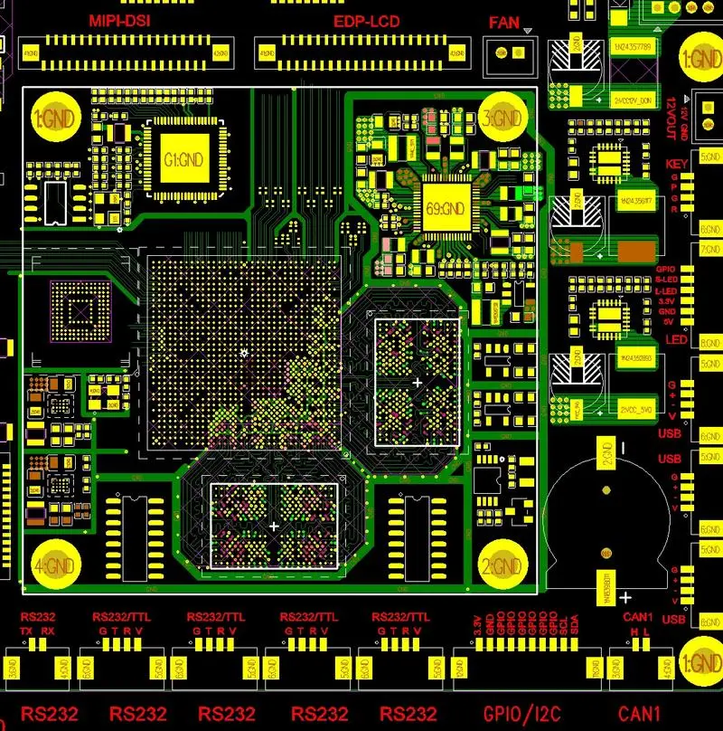
I. Reasonably Divide Functional Zones
When reverse-engineering a schematic from a functional PCB, properly dividing functional zones helps engineers avoid unnecessary complications and improves efficiency. Generally, components with similar functions are placed close together on a PCB. Using functional zones as a basis provides a convenient and reliable reference when extracting the schematic.
However, functional zone division is not arbitrary—it requires a solid understanding of electronic circuits. Start by identifying the core component of a functional block, then trace connections to locate other components within the same functional unit, forming a functional zone. This zoning forms the foundation for schematic extraction. Additionally, make use of component designators (silkscreen labels) on the board—they can significantly speed up the zoning process.
II. Correctly Identify Net Types and Draw Connections
Distinguishing between ground, power, and signal traces requires knowledge of power distribution, circuit connectivity, and PCB routing practices. These traces can be identified by analyzing component connections, copper trace widths, and the characteristics of the electronic product itself.
When drawing connections, use ground symbols extensively to avoid crossing or tangling lines. Use different colors for different net types to maintain clarity. Mark components with standardized symbols, and consider drawing individual circuit blocks separately before combining them into a complete schematic.
III. Identify Reference Components
Reference components serve as anchors when starting the schematic extraction. By basing the drawing on the pins of these reference components, accuracy can be significantly improved.
For experienced engineers, selecting reference components is straightforward. Typically, choose components that play a key role in the circuit—such as integrated circuits, transformers, or transistors—which are often larger in size and have more pins, making them easier to work with.
IV. Understand Basic Frameworks and Leverage Similar Reference Schematics
Engineers should be familiar with the structural frameworks and schematic drawing conventions of basic electronic circuits. This includes being able to directly draw classic, simple circuit blocks and understanding the overall architecture of electronic systems.
Additionally, schematics for similar types of electronic products often share common features. By leveraging experience and referencing comparable circuit diagrams, engineers can accelerate the extraction process for new products.
V. Verification and Optimization
After the schematic is drawn, the reverse-engineering process is not complete until verification and optimization are performed. Components sensitive to PCB parasitic parameters should be reviewed and their nominal values optimized where necessary. The extracted schematic should be compared against the original PCB layout files to ensure full consistency.
One click. One partner. 16 years of expertise: KingshengPCBA delivers full-turnkey PCB/PCBA solutions — from bare boards to box build, with in-house SMT, advanced inspection, and design support.
New customers: 20% off + fast prototyping. Start your free consultation at Kingsheng PCBA.com
With 17 years of expertise in PCBA design, manufacturing, and service, Kingsheng PCBA is ready to help turn your ideas into reality. Feel free to contact us anytime to discuss your requirements and get a professional quotation.
Please send Email to kspcba@c-alley.com or call us through +86 13828766801 Or submit your inquiry by online form. Please fill out below form and attach your manufacturing files( PCB Gerber files and BOM List) if need quotation. We will contact you shortly.
 +86 13828766801
 kspcba@c-alley.com
 https://www.kingshengpcba.com/
 2/F, Building 6, Tangtou 3rd Industrial Zone, Tangtou Community, Shiyan Town, Baoan District, Shenzhen, China, 518108
We would also like to thank our customers for their trust and support. The company's outstanding achievements are mainly due to the loyalty of our customers, which also encourages and spurs our company to forge ahead.