* On your first PCB Assembly order!
* Up to $300 discount
 C - A L L E Y
 Home | Events | PCB | About Us | News | Contact Us
The industrial environment is nothing short of a "trial by fire" for PCBs. With strong electromagnetic interference, extreme temperature fluctuations, high-power motor start-stop cycles, high-voltage electrical arcing, and long-distance signal transmission, these harsh conditions place extreme demands on a PCB's electromagnetic interference (EMI) immunity. When EMI issues arise in industrial equipment, the consequences can range from sensor data anomalies and control system misoperations to production line shutdowns, equipment damage, and even safety incidents—leading to significant economic losses.
The electromagnetic environment for industrial PCBs is fundamentally different from that of consumer electronics. Interference in consumer devices primarily originates from within the system, whereas industrial applications are subject to substantial external interference. High-power variable frequency drives, servo motors, and contactors generate intense electromagnetic radiation and conducted interference; high-voltage lines and welders produce arcing that creates broadband noise; and long signal cables act like antennas, picking up external disturbances. At the same time, industrial PCBs often need to process both high-power signals and small analog signals simultaneously, resulting in a wide current range and disparate signal speeds. The combination of internal and external interference makes EMI suppression far more challenging than in standard PCBs. Under these conditions, ordinary ground plane copper pours are no longer sufficient—a comprehensive reinforcement strategy must be adopted across four dimensions: ground plane structure, thickness, layout, and manufacturing processes.
1. Thick Copper Foil with a Full Solid Ground Plane – Drastically Reducing Ground Impedance
The first cornerstone of industrial PCB ground plane design is the use of thickened copper foil to create a large, continuous ground plane that minimizes ground impedance. Industrial circuits often carry high currents—especially in power and driver modules where transient currents can reach several amperes. Standard 1-oz copper planes can introduce significant ground bounce noise and voltage drops, compromising EMI immunity. Industrial-grade PCB designs prioritize 2-oz, 3-oz, or even thicker copper foil. The increased cross-sectional area reduces ground impedance to the milliohm range, effectively eliminating ground bounce caused by high currents while also enhancing thermal dissipation—critical for equipment that operates continuously under heavy loads. Moreover, the ground plane should fully cover the layer, leaving no unnecessary gaps or splits except for mounting holes and mandatory isolation areas, ensuring a completely uninterrupted return path and eliminating any potential for loop radiation.
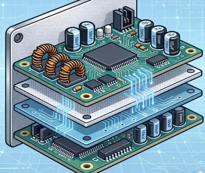
2. Multi-Ground Plane Stack-Up in Multilayer PCBs – Enhancing Shielding and Noise Suppression
A second critical design strategy is the use of a "multi-ground plane" stack-up in multilayer PCBs. Industrial multilayer PCBs typically employ six or more layers with at least two separate ground planes: one designated as the signal ground to serve as the return path and reference for small-signal and analog circuits, and another as the power ground dedicated to handling high-power return currents. This separation isolates high-current noise from sensitive signals. The multiple ground planes also create a double-shielding effect, effectively blocking external electromagnetic radiation from penetrating the PCB while preventing internal noise from radiating outward. For complex industrial PCBs that incorporate analog, digital, power, and RF modules, three or more ground planes can be used—each dedicated to a specific functional domain—to completely eliminate noise coupling between modules.
3. Ground Via Arrays Combined with Chassis Ground – Building a Comprehensive Shielding System
Effective industrial PCB design goes beyond internal ground planes; it also ensures robust bonding between the PCB's ground planes and the equipment chassis, forming an integrated shield of "board-level ground + chassis ground." Dense ground via arrays are placed along board edges, near interface connectors, and around power modules to tie the ground planes directly to the chassis, allowing external interference currents to be shunted safely to the chassis rather than entering the PCB. Additionally, industrial interfaces—such as RS-485, Ethernet, and analog I/O—should incorporate grounding filter circuits that work in conjunction with the ground planes to further attenuate conducted interference. This approach delivers comprehensive EMI suppression across both radiated and conducted paths.
4. Rigid Ground Plane Segregation – Preventing Interference from Mixed High- and Low-Power Circuits
Industrial PCBs often integrate high-power circuits alongside low-level signal circuits. In such cases, the ground planes must be physically separated, with sufficient creepage distance and electrical clearance maintained between the power ground and signal ground. They are connected at only a single point—the system star ground. Similarly, analog and digital grounds should follow partitioning principles to prevent digital noise from contaminating sensitive analog signals. For industrial equipment with explosion-proof or high-safety requirements, the ground plane may also undergo special insulation treatment in line with manufacturing processes to avoid leakage currents and electrostatic discharge (ESD) interference.
Manufacturing Processes: The Key to Reliable Industrial PCB Ground Planes
The effectiveness of industrial PCB ground plane design ultimately depends on manufacturing execution. Standard consumer-grade PCB processes are inadequate to withstand the rigors of industrial environments. Key factors—such as copper foil adhesion, corrosion resistance, high- and low-temperature endurance, and interlayer bond strength—must meet industrial-grade PCB standards. Failure to do so can lead to issues like copper lifting, ground plane discontinuity, or increased impedance over time, resulting in equipment malfunction.
Kingsheng PCBA has years of experience in industrial PCB manufacturing, specializing in high-reliability PCBs and PCBA (printed circuit board assembly) . For industrial PCB ground planes, we utilize thickened electrolytic copper foil and optimized lamination processes to ensure strong adhesion, uniform thickness, and precise control of dielectric and thermal properties. We support customized ground planes from 2 oz to 6 oz copper thickness, with strict adherence to industrial temperature ratings (-40°C to 85°C) . This ensures that our PCBs and PCBAs maintain consistent EMI suppression performance even under the most demanding operating conditions.
With 17 years of expertise in PCBA design, manufacturing, and service, Kingsheng PCBA is ready to help turn your ideas into reality. Feel free to contact us anytime to discuss your requirements and get a professional quotation.

Please send Email to kspcba@c-alley.com or call us through +86 13828766801 Or submit your inquiry by online form. Please fill out below form and attach your manufacturing files( PCB Gerber files and BOM List) if need quotation. We will contact you shortly.
 +86 13828766801
 kspcba@c-alley.com
 https://www.kingshengpcba.com/
 2/F, Building 6, Tangtou 3rd Industrial Zone, Tangtou Community, Shiyan Town, Baoan District, Shenzhen, China, 518108
We would also like to thank our customers for their trust and support. The company's outstanding achievements are mainly due to the loyalty of our customers, which also encourages and spurs our company to forge ahead.


