* On your first PCB Assembly order!
* Up to $300 discount
 C - A L L E Y
 Home | Events | PCB | About Us | News | Contact Us
I.In applications such as photovoltaic power generation, outdoor energy storage, motorhome power supply, industrial equipment and domestic backup power, inverters play a crucial role. Their core function is to convert direct current (DC) into alternating current (AC), providing standard mains power for a wide range of household appliances and industrial equipment. As the control centre and power-handling core of the inverter, the PCBA circuit board directly determines the system’s conversion efficiency, output waveform quality, load stability, safety protection capabilities and service life; it is an indispensable hardware component in new energy power conversion systems.
II.The inverter PCBA integrates a main control MCU chip, an SPWM waveform generation unit, MOSFET power transistors, transformer drive circuits, voltage and current sensing modules, charge management, filtering and voltage regulation, and multiple protection circuits. Low-voltage DC power is input from solar panels and batteries, and is regulated by the PCBA through inversion, step-up conversion and waveform correction, ultimately outputting pure sine-wave AC power capable of driving loads such as air conditioners, refrigerators, motors and office equipment. Whether it be domestic sine-wave inverters, grid-connected photovoltaic inverters or portable outdoor inverters, overall performance is determined by the design and manufacturing standards of the PCBA.
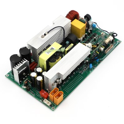
III.Inverters are high-power power electronic devices that operate continuously under heavy loads over extended periods. They face complex operating conditions, including high temperatures, humidity, grid disturbances and frequent load fluctuations, placing far greater demands on the PCBA than ordinary electronic equipment. Substandard PCBAs are prone to unstable output voltage, waveform distortion, poor load-carrying capacity, overheating of the unit and frequent protection-triggered shutdowns. In severe cases, they may even burn out connected equipment, posing a safety hazard.
IV.In terms of circuit design, the inverter PCBA focuses on high-power current-carrying design, isolation between high- and low-voltage circuits, electromagnetic compatibility, and precise waveform control. The power circuit employs thick-copper PCBs and widened high-current traces to reduce line losses and temperature rise; the inverter drive section and signal control section are physically separated and isolated via dedicated routing, with optocouplers used to isolate high- and low-voltage circuits, thereby preventing high-voltage interference with the main control signals. Simultaneously, the SPWM inverter trace layout is precisely optimised and combined with multi-stage filtering circuits to produce a pure sine wave output free from distortion, ensuring no damage to precision household appliances or motor loads. Six built-in protection circuits—overvoltage, undervoltage, overcurrent, short-circuit, overtemperature and overload—automatically cut off the output the moment an anomaly occurs, providing comprehensive protection for both the unit and connected electrical equipment.
V.In terms of materials and manufacturing processes, the high-quality inverter PCBA utilises thick-copper, flame-retardant PCBs with a high glass transition temperature (TG), ensuring resistance to high temperatures and high currents whilst minimising the risk of delamination or deformation. Power MOSFETs, electrolytic capacitors and driver chips are all selected from industrial-grade components with high temperature resistance and low loss, enabling operation across a wide temperature range and ensuring a long service life with excellent resistance to ageing. Production employs a combined SMT and through-hole assembly process, with reinforced soldering of power devices to ensure shock resistance and prevent detachment. The entire board undergoes AOI inspection, full-load ageing tests, high and low-temperature testing, and waveform accuracy checks to strictly control soldering quality and electrical performance. Outdoor PV inverter PCBs generally feature a triple-proof coating, offering dust and moisture resistance, salt spray resistance and weather resistance, making them suitable for long-term operation in open-air environments.
V.With the rapid rise of distributed PV energy, outdoor camping energy storage and power supply for motorhomes, inverters are evolving towards higher frequencies, smaller sizes, greater energy efficiency, smart connectivity and intelligent grid-connection control. This, in turn, is driving continuous iteration of PCBA towards higher power density, higher conversion efficiency, greater integration and enhanced reliability.
VI.The inverter is the heart of new energy power conversion, and the PCBA constitutes the core architecture of this heart. Only through professional circuit layout, robust board materials, comprehensive protection design and mature production processes can inverters achieve high conversion efficiency, pure output waveforms, stable load performance, and safety and durability, thereby providing a solid hardware foundation for photovoltaic power generation, outdoor power supply and industrial backup power.
With 17 years of expertise in PCBA design, manufacturing, and service, KingshengPCBA is ready to help turn your ideas into reality. Feel free to contact us anytime to discuss your requirements and get a professional quotation.
Please send Email to kspcba@c-alley.com or call us through +86 13828766801 Or submit your inquiry by online form. Please fill out below form and attach your manufacturing files( PCB Gerber files and BOM List) if need quotation. We will contact you shortly.
 +86 13828766801
 kspcba@c-alley.com
 https://www.kingshengpcba.com/
 2/F, Building 6, Tangtou 3rd Industrial Zone, Tangtou Community, Shiyan Town, Baoan District, Shenzhen, China, 518108
We would also like to thank our customers for their trust and support. The company's outstanding achievements are mainly due to the loyalty of our customers, which also encourages and spurs our company to forge ahead.