* On your first PCB Assembly order!
* Up to $300 discount
 C - A L L E Y
 Home | Events | PCB | About Us | News | Contact Us
I.In corporate offices, shopping centres, hotels, campuses, industrial parks, factory workshops and whole-home fibre-optic networking scenarios, wireless access points (APs) have become an indispensable part of network infrastructure. They perform vital functions such as transmitting wireless signals, managing user access and providing network signal relay coverage. The PCBA circuit board serves as the core of the wireless AP, directly determining the device’s Wi-Fi coverage range, network speed stability, user capacity, interference resistance and long-term operational lifespan.
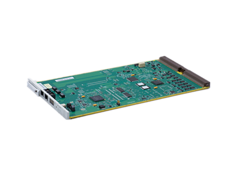
II.The wireless AP PCBA integrates core components such as the main control chip, Wi-Fi RF unit, power amplifier module, Ethernet PHY circuitry, memory and flash storage, power management, and Bluetooth IoT modules. Unlike standard home routers, its core value lies in high-density access, extensive signal coverage and sustained high-load concurrent operation. It can simultaneously support stable connectivity for dozens or even hundreds of mobile phones, computers, surveillance cameras and smart devices, with all these performance capabilities realised through the circuit design and precision manufacturing of the PCBA.
III.Wireless APs are typically installed in corridors, on ceilings or on external walls, where they are often confined in hot, stuffy environments and operate 24 hours a day without interruption, placing extremely high demands on the reliability of the PCBA. Many low-cost APs on the market suffer from issues such as weak signals, frequent disconnections, sluggish internet speeds, insufficient device capacity, and overheating crashes. The root causes are mostly attributed to poor-quality PCB materials, chaotic circuit layouts, non-standard RF routing, and the use of substandard components.
VI.In terms of circuit design, RF signal integrity and electromagnetic compatibility are of paramount importance for wireless AP PCB assemblies. Dual-band and tri-band signals operating at 2.4 GHz, 5 GHz and 6 GHz are extremely sensitive to adjacent routing, which can easily lead to crosstalk and signal attenuation. Professional AP boards employ multi-layer PCB grounding, with RF traces routed along independent paths, strict impedance matching, and equal-length differential pairs. Digital, power supply and RF circuits are physically segregated, effectively reducing electromagnetic interference and ensuring stable WiFi transmission power, excellent wall penetration and consistent network speeds.
V.In terms of materials and manufacturing processes, standard wireless AP PCB assemblies utilise high-TG, high-temperature-resistant, flame-retardant boards that are heat-resistant and resistant to ageing, ensuring they do not delaminate, warp or suffer from solder joint failure under prolonged high-temperature loads. RF, power and main control components are all industrial-grade, high-stability devices capable of operating across a wide temperature range with strong anti-interference capabilities. High-precision SMT assembly is employed, ensuring accurate placement of minute RF components and full, uniform solder joints. AOI and X-ray inspection are conducted to eliminate the risk of cold or missing solder joints. Outdoor wireless AP PCBs also undergo a triple-proof coating process, providing dust and moisture resistance, salt spray resistance, and tolerance to high and low temperatures, making them suitable for harsh outdoor environments.
VI.With the widespread adoption of Wi-Fi 6 and Wi-Fi 7 technologies, coupled with the surge in demand for whole-home fibre-to-the-room (FTTR) networks and high-density wireless coverage in enterprise settings, wireless APs are evolving towards higher integration, tri-band concurrent operation, gigabit and 10-gigabit uplink speeds, low power consumption, and intelligent operation and maintenance. This, in turn, is driving the PCBA to evolve towards more precise routing, enhanced heat dissipation, improved RF isolation, and higher device-carrying capacity.
VII. Although wireless APs may appear simple, their true core capabilities lie within the internal PCBA. Only through excellent circuit layout, robust board materials and components, and mature SMT manufacturing processes can wireless APs achieve uniform signal coverage, prevent lag when multiple devices are online simultaneously, and maintain continuous operation without disconnections over the long term, thereby providing a stable and reliable wireless foundation for enterprise commercial and whole-home smart networks.
With 17 years of expertise in PCBA design, manufacturing, and service, KingshengPCBA is ready to help turn your ideas into reality. Feel free to contact us anytime to discuss your requirements and get a professional quotation.

Please send Email to kspcba@c-alley.com or call us through +86 13828766801 Or submit your inquiry by online form. Please fill out below form and attach your manufacturing files( PCB Gerber files and BOM List) if need quotation. We will contact you shortly.
 +86 13828766801
 kspcba@c-alley.com
 https://www.kingshengpcba.com/
 2/F, Building 6, Tangtou 3rd Industrial Zone, Tangtou Community, Shiyan Town, Baoan District, Shenzhen, China, 518108
We would also like to thank our customers for their trust and support. The company's outstanding achievements are mainly due to the loyalty of our customers, which also encourages and spurs our company to forge ahead.


