* On your first PCB Assembly order!
* Up to $300 discount
 C - A L L E Y
 Home | Events | PCB | About Us | News | Contact Us
In high-speed PCB design, the stack-up structure directly determines signal integrity, electromagnetic compatibility, and manufacturing yield. A poorly designed stack-up introduces impedance discontinuities, crosstalk, and warpage—issues that cannot be fixed by layout alone. Based on over 16 years of manufacturing experience, the following design recommendations provide practical, process-aware guidelines for achieving reliable, high-performance rigid, flex, and rigid-flex PCBs.
1. Stack-up Method
The recommended PCB stack-up method is Foil Stacking.
2. Material Type Control
Minimize the use of different types and models of prepreg (PP) sheets and cores within the same stack-up. The number of PP sheets per dielectric layer shall not exceed three.
3. Dielectric Thickness Control
The thickness of the PP dielectric between two adjacent layers shall not exceed 21 mil.
Note: Thick PP dielectrics are difficult to process and typically require the addition of a core, which increases the total layer count and adds manufacturing cost.
4. Copper Foil Thickness Selection
Note: Copper thickness should be determined based on current carrying requirements and trace width.
5. Symmetrical Stack-up Design
The distribution of routing layers and plane layers shall be symmetrical about the centerline of the stack-up. This includes:
Note: Symmetrical design is essential to prevent warpage and ensure manufacturing reliability. Insulation layer thickness, prepreg type, copper thickness, and pattern type should all be balanced about the centerline.
6. Design Margin for Signal Integrity
Sufficient margin shall be reserved for trace width and dielectric thickness to prevent signal integrity (SI) issues and other reliability concerns caused by insufficient design tolerance.
Layer Type Definition
PCB stack-ups consist of three fundamental layer types:
Application Across PCB Variants
The above stack-up design recommendations apply to the following PCB technologies, with additional considerations as noted:
Rigid PCB
Traditional rigid circuit boards that provide structural strength and mechanical stability. The stack-up guidelines outlined above are directly applicable to rigid PCB designs.
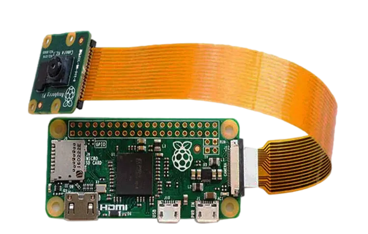
Flex PCB
Flexible circuit boards manufactured from materials such as polyimide, enabling bending and folding applications. When designing flex PCBs, the following additional factors must be considered alongside the core principles:
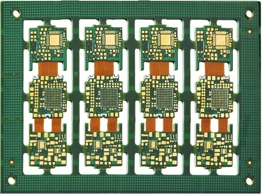
Rigid-Flex PCB
A hybrid construction integrating rigid and flexible circuit sections into a single interconnected structure. Stack-up symmetry must be maintained across the entire assembly, with particular attention to:
With over 16 years of industry-leading expertise, Kingsheng PCBA specializes in high-precision PCBA design and manufacturing. Our deep experience in stack-up optimization, material selection, and process control ensures that every project meets the highest standards of signal integrity, reliability, and manufacturability. Whether rigid, flex, or rigid-flex boards, we deliver professional solutions tailored to your high-speed design requirements.
Partner with Kingsheng PCBA — where experience meets excellence.
With 17 years of expertise in PCBA design, manufacturing, and service, KingshengPCBA is ready to help turn your ideas into reality. Feel free to contact us anytime to discuss your requirements and get a professional quotation.

Please send Email to kspcba@c-alley.com or call us through +86 13828766801 Or submit your inquiry by online form. Please fill out below form and attach your manufacturing files( PCB Gerber files and BOM List) if need quotation. We will contact you shortly.
 +86 13828766801
 kspcba@c-alley.com
 https://www.kingshengpcba.com/
 2/F, Building 6, Tangtou 3rd Industrial Zone, Tangtou Community, Shiyan Town, Baoan District, Shenzhen, China, 518108
We would also like to thank our customers for their trust and support. The company's outstanding achievements are mainly due to the loyalty of our customers, which also encourages and spurs our company to forge ahead.


