* On your first PCB Assembly order!
* Up to $300 discount
 C - A L L E Y
 Home | Events | PCB | About Us | News | Contact Us
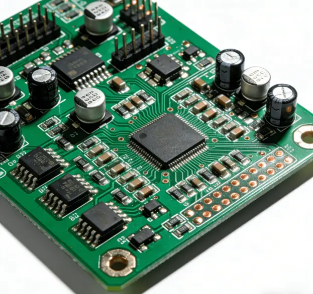
Although semiconductor integration continues to advance, with many applications supported by readily available system-on-chip solutions and feature-rich, off-the-shelf development boards, numerous electronic applications still require custom PCB designs. Even in one-off developments, a well-designed PCB plays a critical role.
The PCB serves as the physical platform for design and represents the most flexible component for building electronic systems using discrete components. This article introduces several golden rules of PCB design—rules that have remained largely unchanged since the advent of commercial PCB design 25 years ago. These principles apply broadly across PCB design projects and offer valuable guidance for both young electronic design engineers and experienced circuit board manufacturers alike. The following content outlines ten of the most effective design rules that electronic design engineers should keep in mind and practice when using design software for PCB layout and preparing for commercial manufacturing. Engineers need not follow these rules in chronological order or by relative importance; simply adhering to all of them can significantly improve product design.
1. Choose the Correct Grid
Set and consistently use a grid spacing that matches the majority of components. While multiple grids may seem advantageous, engineers who invest time in thoughtful planning during the early stages of PCB layout can avoid spacing challenges and maximize board utilization. Since many components are available in various package sizes, engineers should use the grid that best suits their design. Additionally, polygons are critical for copper pours on circuit boards. Multi-grid PCBs often result in polygon fill deviations—though less standard than single-grid approaches—which can provide more than adequate board longevity.
2. Keep Paths Short and Direct
This principle may sound simple and obvious, but it should be kept in mind at every stage—even if it means modifying the board layout to optimize routing lengths. This is especially critical for analog and high-speed digital circuits, where system performance is often partially constrained by impedance and parasitic effects.
3. Use Power Planes to Manage Power and Ground Distribution
Power plane copper pours are a fast and straightforward option in most PCB design software. By providing a common connection for a large number of conductors, this approach ensures efficient current delivery with minimal impedance or voltage drop, while also offering sufficient return paths for ground. Where possible, multiple power supply traces can be routed within the same board area, and it is advisable to ensure that the ground plane covers most of a given layer, which helps manage interactions between traces on adjacent layers.
4. Group Related Components Together with Required Test Points
Place discrete components associated with a given functional block—such as the passive components for an operational amplifier (op-amp)—close to the device. This allows bypass capacitors and resistors to work in close coordination, helps optimize routing lengths as mentioned in Rule 2, and simplifies testing and fault detection.
5. Panelize the Board by Replicating the Design Multiple Times
Select a panel size that aligns with the manufacturer's preferred equipment dimensions to reduce prototyping and production costs. Begin by arranging the board layout on a panel, consult with the circuit board manufacturer to obtain their preferred panel dimensions, then modify your design specifications to repeat the board layout multiple times within those panel dimensions.
6. Consolidate Component Values
As a designer, you may encounter discrete components that offer similar performance but with varying values. By consolidating these into a smaller range of standard values, you can simplify the bill of materials (BOM) and potentially reduce costs. If you develop a range of PCB products based on preferred component values, this approach also supports better long-term inventory management decisions.
7. Perform Design Rule Checks (DRC) as Often as Possible
Although running DRC functions in PCB software takes only a short amount of time, performing checks consistently throughout the design process can save significant time in complex design environments. This is a good habit to maintain. Every routing decision matters, and DRC serves as an ongoing reminder of the most critical routing requirements.
8. Use Silkscreen Flexibly
Silkscreen can be used to label a variety of useful information for future reference by board fabricators, service or test engineers, assemblers, or equipment debuggers. Clearly label functional blocks and test points, and wherever possible, indicate component and connector orientations—even if such annotations are printed on the underside of the board (under components, after assembly). Applying silkscreen thoughtfully on both the top and bottom layers can reduce rework and streamline the production process.
9. Always Include Decoupling Capacitors
Do not attempt to optimize your design by omitting power line decoupling and relying solely on component datasheet limits. Capacitors are inexpensive and robust. Invest time in properly placing decoupling capacitors, and follow Rule 6 by using standard value ranges to maintain inventory consistency.
10. Generate PCB Manufacturing Parameters and Verify Before Production
Although most circuit board manufacturers are willing to download and verify files on your behalf, it is good practice to generate Gerber files yourself and review them using a free viewer to ensure they match your expectations. This helps avoid misunderstandings. By performing your own verification, you may also catch inadvertent errors, preventing costly production runs based on incorrect parameters.
Conclusion
As circuit design becomes increasingly collaborative and internal teams rely more heavily on reference designs, foundational principles such as those outlined above will remain a defining feature of printed circuit board design. We believe these principles are essential to PCB design. By following these fundamental rules, developers gain the flexibility to enhance product value and maximize the benefits derived from the boards they manufacture. Even newcomers to circuit board design can accelerate their learning curve and build confidence by keeping these essential rules in mind.
With over 17 years of industry-leading expertise, KingshengPCBA specializes in high-precision PCBA design and manufacturing. Our deep experience in PCB layout optimization, signal integrity, and manufacturability ensures that every project meets the highest standards of quality and reliability. Whether you are developing prototypes or preparing for mass production, we deliver professional solutions tailored to your design requirements..

Please send Email to kspcba@c-alley.com or call us through +86 13828766801 Or submit your inquiry by online form. Please fill out below form and attach your manufacturing files( PCB Gerber files and BOM List) if need quotation. We will contact you shortly.
 +86 13828766801
 kspcba@c-alley.com
 https://www.kingshengpcba.com/
 2/F, Building 6, Tangtou 3rd Industrial Zone, Tangtou Community, Shiyan Town, Baoan District, Shenzhen, China, 518108
We would also like to thank our customers for their trust and support. The company's outstanding achievements are mainly due to the loyalty of our customers, which also encourages and spurs our company to forge ahead.


