* On your first PCB Assembly order!
* Up to $300 discount
 C - A L L E Y
 Home | Events | PCB | About Us | News | Contact Us
As the semiconductor industry enters the "post-Moore" era, traditional transistor scaling faces physical limits. Advanced packaging, especially wafer-level packaging (WLP), has become a key enabler for continued performance gains and miniaturization. For PCBA manufacturers, mastering WLP assembly is no longer an option but a necessity to serve high-density, miniaturized electronic products.
I. What is WLP and Why Does It Matter?
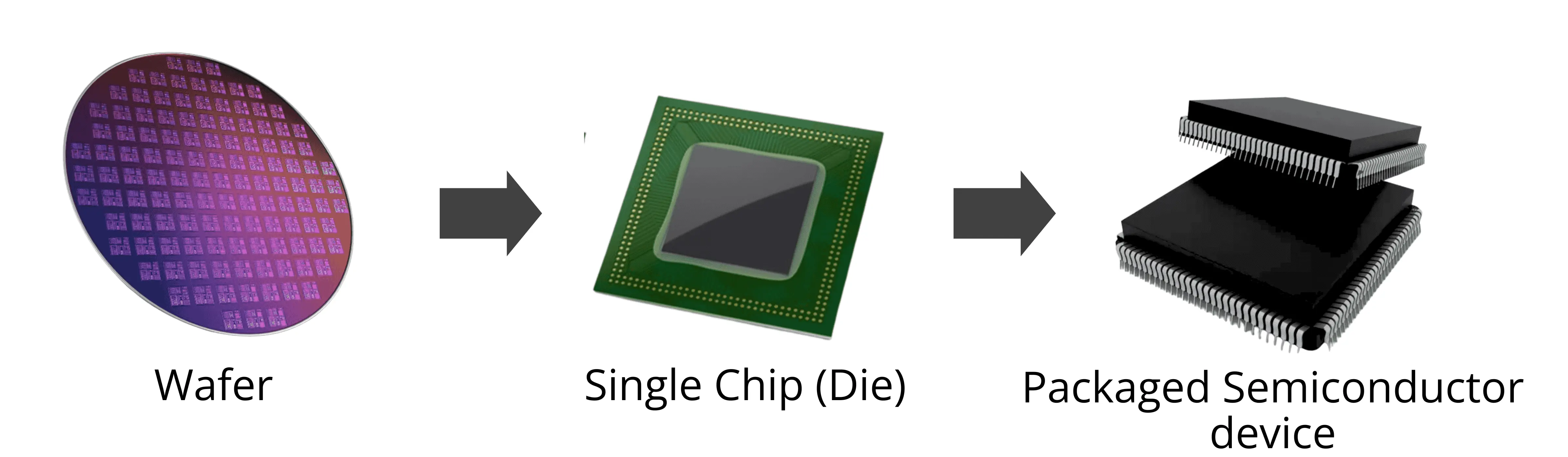
Wafer-level packaging performs packaging processes at the wafer level before dicing. The resulting package is nearly the same size as the silicon die, hence also known as wafer-level chip-scale packaging (WLCSP). Compared with conventional packaging, WLP offers several advantages: ultra-small form factor, higher I/O density, superior electrical performance (shorter signal paths, lower parasitic inductance and capacitance), shorter cycle times, and lower cost.
WLP is divided into two main categories. Fan-in WLP keeps all I/O terminals within the die area, suitable for low-pin-count devices such as power management ICs, RF transceivers, and microcontrollers. Fan-out WLP redistributes I/O beyond the die edge, enabling higher I/O density and heterogeneous integration. It is widely used in smartphones, wearables, MEMS sensors, and high-performance computing.
II. Critical Assembly Process for WLP on PCBA
Although WLP components are supplied in tape-and-reel and can be assembled using standard SMT equipment, several process steps demand special attention.
1. PCB pad design – Two pad types exist: solder mask defined (SMD) and non-solder mask defined (NSMD). In practice, NSMD pads are preferred for WLP because they provide more accurate pad dimensions and better solder joint reliability.
2. Solder paste deposition and stencil design – Ultra-fine pitches (≤0.15 mm) challenge the printing process. A high-quality laser-cut stainless steel stencil with a nano-coating significantly improves transfer efficiency and consistency, especially for pitches below 0.4 mm.
3. Pick and placement – WLP uses flip-chip technology, placing the active side of the die toward the PCB. The bumps form both electrical and mechanical connections in one step. Precision placement equipment with plastic pickup nozzles is required to handle these fine-pitch devices.
4. Reflow soldering – A three-zone reflow profile is critical: preheat (80-120 °C), soak (150-180 °C), and peak (240 °C). Oxygen content should be kept between 10-30 ppm, and the cooling rate controlled at 5-8 °C/s to ensure robust solder joints.
5. Inspection – Solder paste inspection (SPI) and automated optical inspection (AOI) are strongly recommended. Most WLP devices are rated JEDEC MSL 1, so pre-assembly baking is typically unnecessary.
III. Common Challenges and Practical Solutions
1. Warpage control – CTE mismatch between the silicon die and PCB can cause substrate warpage during reflow, leading to opens or shorts. The solution is to perform simulation-based warpage prediction before assembly and adjust stencil design and reflow profiles accordingly.
2. Bumping process – For bumps with a pitch above 0.5 mm, a ball-dropper method is efficient. For 0.3-0.5 mm pitch, a stencil-based method works well. Below 0.3 mm, high-precision solder paste printing must be employed.
3. Environment control – When ambient temperature exceeds 28 °C, solder paste viscosity drops and bump shift increases by up to 30%. Therefore, the assembly environment should be strictly maintained at 22 ± 2 °C.
IV. Equipment Capability: The Backbone of WLP Assembly
Successful WLP assembly requires high-precision placement machines, fine-pitch stencils with nano-coating, and advanced bumping equipment. For instance, high-accuracy ball placement systems can achieve a bridge defect rate below 0.8% for 0.3 mm pitch devices, with ball shear strength reaching 42 N. Investing in such capabilities is essential for any PCBA factory targeting advanced packaging applications.
V. Market Outlook
According to QYResearch, the global WLP market was valued at approximately US 4.72 billionin2025andisprojectedtoreachUS 4.72 billionin2025andisprojectedtoreachUS 9.04 billion by 2032, growing at a CAGR of 9.7%. Driven by AI, high-performance computing, and consumer electronics miniaturization, WLP has become a major growth engine.
VI. Conclusion
As electronics continue to shrink and integrate, the adoption of wafer-level packaging will only accelerate. From fan-in to fan-out, from single-die to multi-die heterogeneous integration, the requirements for precision, stability, and reliability are rising. PCBA factories must continuously optimize their process parameters, upgrade equipment, and strengthen quality control systems to build a competitive edge in WLP assembly.
Our PCBA factory has fully mastered the WLP precision assembly process. Equipped with fine-pitch placement systems and an experienced engineering team, we are ready to support your most demanding miniaturization projects. Contact us to discuss your WLP assembly needs.
With 17 years of expertise in PCBA design, manufacturing, and service, KingshengPCBA is ready to help turn your ideas into reality. Feel free to contact us anytime to discuss your requirements and get a professional quotation.

Please send Email to kspcba@c-alley.com or call us through +86 13828766801 Or submit your inquiry by online form. Please fill out below form and attach your manufacturing files( PCB Gerber files and BOM List) if need quotation. We will contact you shortly.
 +86 13828766801
 kspcba@c-alley.com
 https://www.kingshengpcba.com/
 2/F, Building 6, Tangtou 3rd Industrial Zone, Tangtou Community, Shiyan Town, Baoan District, Shenzhen, China, 518108
We would also like to thank our customers for their trust and support. The company's outstanding achievements are mainly due to the loyalty of our customers, which also encourages and spurs our company to forge ahead.


