* On your first PCB Assembly order!
* Up to $300 discount
 C - A L L E Y
 Home | Events | PCB | About Us | News | Contact Us
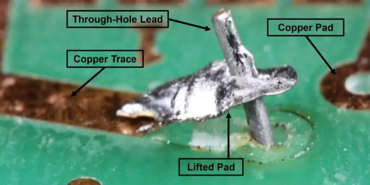
In PCBA manufacturing, pad lifting (or pad cratering) is one of the most frustrating quality failures. A board passes electrical test and SMT inspection, yet fails in the field due to a detached pad. The hidden culprit? Copper foil adhesion – the bond strength between the copper pad and the PCB base material.
Understanding this relationship is critical for any PCBA factory that claims high reliability. Let's explore the failure mechanism and how systematic process control prevents pad lifting before it happens.
I. The Root Cause: Insufficient Adhesion Strength
Pad lifting occurs when the copper foil's peel strength falls below the stress applied during assembly or operation. IPC-6012 specifies a minimum peel strength of 1.0 N/mm for standard FR-4 boards. Below 0.8 N/mm, the risk of pad separation under thermal shock (reflow, wave soldering, or rework) increases dramatically.
The failure originates at the copper-to-resin interface. Two factors govern adhesion:
1. Mechanical anchoring – surface roughness of the copper foil (oxide treatment)
2. Chemical bonding – coupling agents between copper and resin
If the PCB supplier uses poor surface roughening, uneven oxide layers, or degraded coupling agents, the bond strength is compromised even before assembly. Additionally, low-Tg resin or incomplete curing can cause interfacial strength to drop sharply at elevated temperatures.
II. The Failure Chain: From Incoming Material to Assembly
Pad lifting rarely has a single cause. It is a chain of issues:
1. PCB incoming quality – substandard copper foil roughness, insufficient resin curing, or low Tg material. Case analysis shows BGA pad cratering after rework often traced back to improper lamination parameters and low Tg resin.
2. PCB fabrication – over-etching weakens pad edge structure; improper lamination pressure/temperature reduces cross-linking density.
3. PCBA assembly – excessive peak reflow temperature (>260°C) or prolonged liquidus time (>90s) adds thermal stress. Multiple rework cycles further accumulate damage.
III. Special Risk: ENIG "Black Pad" Phenomenon
For ENIG (Electroless Nickel Immersion Gold) surface finish, an additional adhesion killer exists: black pad. When nickel bath parameters (temperature, pH) drift or immersion gold time is too long, the nickel layer becomes excessively corroded, forming a dark, rough, porous structure.
Black pad does not affect gold appearance; it reduces solderability and joint strength dramatically. Failures are insidious – boards pass initial test but crack after thermal cycling or mechanical shock in the field. A professional PCBA factory must require nickel phosphorus content (10-12% for medium phosphorus) and process control records from its PCB suppliers.
IV. How a Reliable PCBA Factory Prevents Pad Lifting
Systemic prevention is the only solution. Here are the essential controls:
1. Material qualification
Request peel strength test reports from PCB suppliers (≥1.0 N/mm).
For high-reliability projects, perform thermal stress validation (288°C solder dip for 10s, then check for lifting/blistering).
For ENIG, require XRF thickness data and nickel bath logs.
2. Process optimization
Reflow ramp rate ≤3°C/s to avoid thermal shock.
Peak temperature matched to PCB Tg rating; liquidus time 60-90s for lead-free.
For rework, use constant-temperature soldering tools, limit heating to 3-5s per pad, and avoid multiple cycles.
3. Reliability verification
Conduct regular pad pull/shear tests on process coupons.
Perform thermal cycling (-40°C ↔ 125°C, 100 cycles) on sample batches.
Use X-ray inspection to detect BGA pad anomalies before assembly.
4. Full traceability
Implement MES (Manufacturing Execution System) linking incoming PCB data, reflow profiles, and test outcomes. This enables rapid root-cause analysis when defects appear.
V. Conclusion
Pad lifting is not a "rework it and ship it" problem. It is the result of weak copper adhesion combined with uncontrolled thermal stress. A professional PCBA factory adds value by managing the entire chain – from qualified PCB materials and precise reflow profiling to ongoing reliability testing.
Choosing a PCBA partner that understands copper foil adhesion and proactively prevents pad lifting is the key to delivering electronics that survive real-world thermal and mechanical demands. Don't let a lifted pad become your customer's first failure.
With 17 years of expertise in PCBA design, manufacturing, and service, KingshengPCBA is ready to help turn your ideas into reality. Feel free to contact us anytime to discuss your requirements and get a professional quotation.

Please send Email to kspcba@c-alley.com or call us through +86 13828766801 Or submit your inquiry by online form. Please fill out below form and attach your manufacturing files( PCB Gerber files and BOM List) if need quotation. We will contact you shortly.
 +86 13828766801
 kspcba@c-alley.com
 https://www.kingshengpcba.com/
 2/F, Building 6, Tangtou 3rd Industrial Zone, Tangtou Community, Shiyan Town, Baoan District, Shenzhen, China, 518108
We would also like to thank our customers for their trust and support. The company's outstanding achievements are mainly due to the loyalty of our customers, which also encourages and spurs our company to forge ahead.


