* On your first PCB Assembly order!
* Up to $300 discount
 C - A L L E Y
 Home | Events | PCB | About Us | News | Contact Us
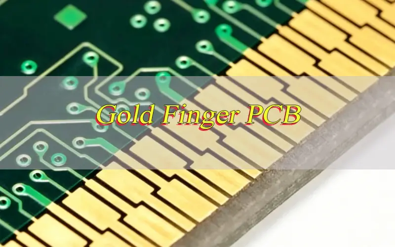
In PCBA manufacturing, gold fingers are the critical interface between a board and its connector. Their reliability determines product lifespan and signal integrity. Yet many designers and procurement professionals fall into dangerous myths about gold plating thickness – leading to contact failure, wear, and even scrap. Here are the most common misconceptions and how a professional PCBA factory avoids them.
Myth 1: "Thicker gold is always better"
This is the most widespread and harmful belief. Some specify gold thickness up to 2.0μm or more, assuming it guarantees higher durability. In reality, hard gold (gold-cobalt or gold-nickel) beyond ~1.3μm increases internal stress, causing micro-cracks and peeling during insertion. Excess gold also changes mating clearance, raising insertion force and damaging elastic contacts. Worse, it adds 30–50% unnecessary cost. The correct approach: 0.4–0.5μm for <100 cycles, 0.76μm for 100–500 cycles, and 1.0–1.3μm for >500 cycles.
Myth 2: Ignoring the nickel underlayer
Failure analysis often shows gold still present but high contact resistance. Cross-section reveals the real problem: a nickel layer that is too thin (<2μm), too porous, or mismatched in hardness. Nickel acts as a diffusion barrier and support. With thin nickel, copper atoms migrate through pores to the gold surface, forming copper oxides that block conduction. Some factories try to hide thin nickel with extra gold – but after a few insertions, the underlayer fails. The standard: nickel thickness ≥3μm, low stress, low porosity.
Myth 3: Average thickness passes, but edges are too thin
XRF measurement often reports an average gold thickness of 0.5μm – compliant. However, edges, tips, and corners of the gold finger may have only 0.2μm due to uneven current distribution during electroplating. These weak points wear first, exposing nickel or copper, leading to corrosion and contact failure. A professional PCBA factory requires cross-section micrographs measuring at least five points (including chamfer start, center, and edges), not just XRF averages.
Myth 4: Confusing hard gold with soft gold (ENIG)
Another fatal mistake: using ENIG (electroless nickel immersion gold, a.k.a. soft gold) for gold fingers that require frequent insertion. ENIG deposits pure gold (soft, >99.9% purity) at 0.05–0.1μm thickness. It offers no wear resistance. One insertion scratches it off, exposing black nickel, and contact fails immediately. Gold fingers must use electroplated hard gold (with 0.1–0.3% cobalt or nickel, 130–200 HV). Drawings must explicitly state "Hard Gold over Nickel" with thickness and hardness requirements. Never substitute ENIG for hard gold.
Myth 5: Ignoring copper roughness and nickel flatness
Plating thickness is an absolute value, but rough copper surfaces consume effective wear thickness. If the copper under gold fingers has Ra > 0.5μm, the nickel and gold layers follow the peaks and valleys. The peaks get much thinner real coverage and wear through first. A professional factory polishes or micro-etch the gold finger area to Ra ≤ 0.2μm before nickel plating, ensuring uniform thickness translates into real durability.
How a professional PCBA factory avoids these pitfalls
1. Process control – Measure incoming copper roughness; use dedicated fixtures and auxiliary cathodes for uniform electroplating; perform cross-section analysis on every batch.
2. Testing capability – Use calibrated XRF plus cross-sectioning to report thickness at edges, corners, and flat areas. For high-reliability products, add insertion durability and contact resistance tests.
3. Process expertise – Keep ENIG and electroplated hard gold lines separate. Recommend optimum stack-up (e.g., 5μm nickel + 1.0μm hard gold) based on insertion cycles and environment (salt spray, humidity, temperature).
Conclusion
Gold finger plating thickness is not "the thicker the better," nor is "average thickness" enough. From nickel integrity, proper hard gold range, edge coverage to surface roughness – every misconception leads to insertion failure. During NPI, designers and process engineers should review gold finger specifications against IPC-4552 (for ENIG) or customer hard gold standards, and validate with reliability testing. Avoid these common myths, and your product will maintain reliable connections through thousands of insertions.
With 17 years of expertise in PCBA design, manufacturing, and service, Kingsheng PCBA is ready to help turn your ideas into reality. Feel free to contact us anytime to discuss your requirements and get a professional quotation.

Please send Email to kspcba@c-alley.com or call us through +86 13828766801 Or submit your inquiry by online form. Please fill out below form and attach your manufacturing files( PCB Gerber files and BOM List) if need quotation. We will contact you shortly.
 +86 13828766801
 kspcba@c-alley.com
 https://www.kingshengpcba.com/
 2/F, Building 6, Tangtou 3rd Industrial Zone, Tangtou Community, Shiyan Town, Baoan District, Shenzhen, China, 518108
We would also like to thank our customers for their trust and support. The company's outstanding achievements are mainly due to the loyalty of our customers, which also encourages and spurs our company to forge ahead.


