* On your first PCB Assembly order!
* Up to $300 discount
 C - A L L E Y
 Home | Events | PCB | About Us | News | Contact Us
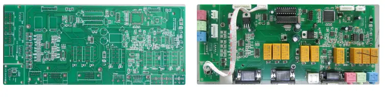
In the PCBA process, the prototyping phase is critical for validating design feasibility. If manufacturability issues are not identified during this phase, they will directly lead to lower yields, delayed delivery, and increased costs in mass production. As an operator of an independent website, we have observed that many customers repeatedly modify their designs during prototyping. The root cause is the lack of a systematic method to quickly assess manufacturability issues. This article organizes the most efficient inspection points during prototyping from two dimensions: bare PCB fabrication and SMT assembly.
I. Quick Checks at the Bare PCB Level
1. Minimum Trace Width and Spacing
Verify whether the minimum trace width and spacing in the design files meet the factory’s process capabilities. For standard prototyping, the minimum trace width and spacing are typically 4 mils (0.1 mm). Values below this require confirmation that the factory has the corresponding etching and compensation capabilities. Quick method: measure the spacing in the densest area of the Gerber files, or directly check the factory’s parameter sheet.
2. Annular Ring and Via Size
Check the width of the annular ring. Within the allowable tolerance of drill offset, the annular ring width should be at least 50% of the drill diameter. For example, if the drill diameter is 0.3 mm, the outer diameter of the annular ring should be no less than 0.45 mm. For via size, the minimum mechanical drill diameter is typically 0.2 mm. Smaller diameters require laser drilling, which significantly increases prototyping time and cost.
3. Solder Mask Dam
For ICs with a pin pitch of 0.5 mm or less (e.g., QFP, QFN packages), check whether a solder mask dam is preserved between adjacent pads. If the pad spacing is less than 0.1 mm, a solder mask dam cannot be formed, leading to solder bridging risks. Quick method: measure the distance between the edges of adjacent pads in CAM software.
II. Quick Checks at the SMT Assembly Level
1. Component Spacing and Orientation
Ensure sufficient clearance is maintained between adjacent components for placement. For 0402 and larger chip resistors and capacitors, the component spacing should be at least 0.3 mm. The orientation of polarized components (diodes, tantalum capacitors, ICs) should be uniform to avoid frequent nozzle rotation by the pick-and-place machine. Quick method: check the orientation consistency of the same component types in the layout files.
2. Reworkability of BGA and QFN
For BGA packages, reserve at least 1.5 mm of component-free area around the periphery for hot air rework nozzles. For QFN packages, the side thermal pads should be exposed to allow access for manual soldering. Without these areas, soldering defects during prototyping cannot be reworked.
3. Test Points and Panelization Rails
Check whether test points are preserved. Each critical power net and signal net should have at least one exposed pad with a diameter of 1.0 mm or larger for ICT or flying probe testing. For panelized designs, confirm that the V-cut or mouse bite locations are in areas without components, and that the rail width is greater than 5 mm.
III. Quick Checks at the File and Data Level
1. Drill File and Layer Alignment
Overlay the drill file with each copper layer and check whether the drill center aligns with the pad center. Misalignment exceeding 20% of the drill diameter indicates registration issues. Quick action: use free tools such as Gerbv or ViewMate to import all layers, zoom in on drill areas, and verify one by one.
2. Solder Mask Opening and Pad Matching
The solder mask opening should be 0.05–0.1 mm larger than the pad on each side. Excessive openings lead to missing solder mask between pads, while insufficient openings cover part of the pad and affect soldering. Quick method: overlay the solder mask layer with the paste mask layer and check whether the opening edges fully enclose the pads.
3. Silkscreen Overlap with Pads
Silkscreen text must not fall on pads or copper surfaces, as the ink can become a contaminant during reflow. Quick check: select the silkscreen layer and the pad layer, and visually identify any overlapping areas.
Conclusion
The above inspection items can be completed within 30 minutes and are suitable for pre-prototyping self-checks or for EQ confirmation with the factory. The cost of identifying and correcting most manufacturability issues during the prototyping phase is less than 5% of the cost of correcting them during mass production. Mastering this rapid assessment method can effectively reduce prototyping iterations and allow more focus on product functionality validation.
With 17 years of expertise in PCBA design, manufacturing, and service, KingshengPCBA is ready to help turn your ideas into reality. Feel free to contact us anytime to discuss your requirements and get a professional quotation.

Please send Email to kspcba@c-alley.com or call us through +86 13828766801 Or submit your inquiry by online form. Please fill out below form and attach your manufacturing files( PCB Gerber files and BOM List) if need quotation. We will contact you shortly.
 +86 13828766801
 kspcba@c-alley.com
 https://www.kingshengpcba.com/
 2/F, Building 6, Tangtou 3rd Industrial Zone, Tangtou Community, Shiyan Town, Baoan District, Shenzhen, China, 518108
We would also like to thank our customers for their trust and support. The company's outstanding achievements are mainly due to the loyalty of our customers, which also encourages and spurs our company to forge ahead.


