* On your first PCB Assembly order!
* Up to $300 discount
 C - A L L E Y
 Home | Events | PCB | About Us | News | Contact Us
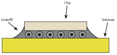
As electronic products continue to evolve toward miniaturization, high density, and high reliability, the risk of stress-related failures in PCBA manufacturing has increased significantly. Underfill, an adhesive material filled into the gap between a chip and a substrate, effectively dissipates thermal stress and mechanical shock, preventing solder joint cracks. For PCBA manufacturers, correctly identifying the application scenarios of underfill and setting appropriate process parameters are key measures to improve product yield and long-term reliability.
I. Main Application Scenarios of Underfill
1. Handheld and Mobile Devices
Smartphones, tablets, smartwatches, and similar devices frequently experience drops, vibrations, and temperature changes. Underfill is primarily used to protect solder joints in BGA and CSP packages. For example, in accelerometers, power management chips, and RF modules, underfill can increase drop shock resistance by three to five times.
2. Automotive Electronic Systems
Engine control units, ADAS camera modules, and in-vehicle infotainment systems operate for extended periods under high temperature, vibration, and humidity cycling. Underfill eliminates shear stress caused by mismatches in the coefficient of thermal expansion between the chip and the substrate, preventing solder joint failure due to thermal cycle fatigue.
3. Medical and Industrial Electronics
Implantable medical devices, industrial sensors, and security surveillance equipment require continuous long-term operation without solder joint fractures. Underfill is used in these scenarios primarily to protect high-value or difficult-to-repair modules, such as microprocessors, FPGAs, and RF front-end modules.
4. Flexible and Rigid-Flex Boards
In flexible areas, solder joints of rigid devices experience repeated stress during bending. Underfill limits the deformation at the edges of component solder joints, reducing the risk of copper foil cracking. Common applications include wearable devices and connector boards in foldable phones.
II. Key Process Parameter Settings for Underfill
1. Preheating Parameters
Preheating temperature is typically set between 80 and 120 degrees Celsius for 30 to 60 seconds. The purpose of preheating is to reduce adhesive viscosity and minimize temperature differences across the substrate surface, preventing bubbles caused by local cooling during adhesive flow. After preheating, the substrate surface temperature should be uniform, with a temperature difference controlled within 10 degrees Celsius.
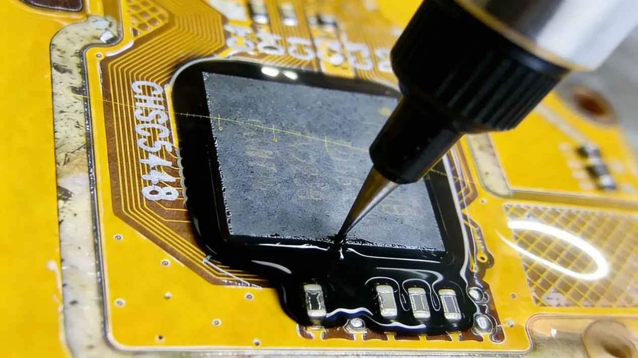
2. Dispensing Path and Speed
A single-sided or L-shaped dispensing path is suitable for small-sized chips. Dispensing speed is recommended at 2 to 5 millimeters per second. The adhesive volume is calculated based on chip volume multiplied by the fill gap percentage, typically 70% to 90% of the gap volume between the chip and the substrate. Excessive speed may generate bubbles, while insufficient speed reduces production efficiency.
3. Capillary Flow Wait Time
Allow 15 to 30 seconds after dispensing for the adhesive to naturally fill the entire gap using capillary effect. No external force or airflow should be applied during this stage. If the chip size exceeds 10 millimeters by 10 millimeters, consider extending the wait time to more than 45 seconds.
4. Curing Temperature and Time
Common curing temperature ranges from 120 to 150 degrees Celsius for 5 to 15 minutes. Low-temperature curing adhesives can be used at 80 to 100 degrees Celsius, but the curing time should be extended to 20 to 30 minutes. The ramp rate should be controlled at 2 to 4 degrees Celsius per second to avoid thermal shock that could cause delamination of the chip or substrate.
5. Key Inspection Parameters
After curing, the fill coverage must be measured and required to reach above 95%. Perform cross-section or acoustic scanning at the four corners and the center of the chip to confirm the absence of continuous voids. Residual adhesive must not contaminate adjacent connectors, test points, or gold finger areas.
III. Common Process Defects and Parameter Adjustment Directions
1. Incomplete Fill
Manifested as adhesive not fully spreading to the opposite side at the chip edge. The solution is to increase the preheating temperature by 5 to 10 degrees Celsius or extend the wait time by 10 to 15 seconds. If not improved, switch to a lower-viscosity underfill adhesive.
2. Concentrated Voids
Voids appear in the center or at the four corners of the chip. Center voids are often caused by excessive preheating temperature leading to premature curing; reduce the preheating temperature by 10 degrees Celsius. Corner voids are usually due to insufficient adhesive volume; increase the single dispensing volume by 10% to 15%.
3. Chip Shift
The chip shifts position after curing, commonly seen in large packages. Reduce the ramp rate to 1 to 2 degrees Celsius per second, or add a light pressure block of 50 to 100 grams before curing.
IV. Process Validation and Documentation Requirements
After each change of adhesive batch or equipment parameters, produce at least five test boards for destructive cross-sectional analysis. Record preheating temperature, dispensing speed, curing profile, and fill rate. Process parameter documentation should include normal operating ranges and alarm limits, for example, automatically stopping production when the curing temperature deviation exceeds plus or minus 5 degrees Celsius.
Underfill application is not necessary for every PCBA. However, for high-reliability scenarios, correct underfill process parameter settings directly determine product lifespan in field use. Independent website operators can use the above parameters as foundational content for customer technical consultations, helping customers identify whether their own products require the introduction of underfill processes.
With 17 years of expertise in PCBA design, manufacturing, and service, KingshengPCBA is ready to help turn your ideas into reality. Feel free to contact us anytime to discuss your requirements and get a professional quotation.

Please send Email to kspcba@c-alley.com or call us through +86 13828766801 Or submit your inquiry by online form. Please fill out below form and attach your manufacturing files( PCB Gerber files and BOM List) if need quotation. We will contact you shortly.
 +86 13828766801
 kspcba@c-alley.com
 https://www.kingshengpcba.com/
 2/F, Building 6, Tangtou 3rd Industrial Zone, Tangtou Community, Shiyan Town, Baoan District, Shenzhen, China, 518108
We would also like to thank our customers for their trust and support. The company's outstanding achievements are mainly due to the loyalty of our customers, which also encourages and spurs our company to forge ahead.


