* On your first PCB Assembly order!
* Up to $300 discount
 C - A L L E Y
 Home | Events | PCB | About Us | News | Contact Us
As core components in fiber-optic communication systems, optical modules perform the conversion between electrical and optical signals. With increasing bandwidth demands from data centers, 5G base stations, and high-speed transmission networks, optical module data rates are evolving from 25G and 100G toward 400G and 800G. The placement accuracy of optical module PCBAs (Printed Circuit Board Assemblies) directly determines signal integrity, anti-interference capability, and long-term reliability. The following explains three key dimensions of high-precision placement.
I. Unique Characteristics of Optical Module PCBAs Demand Higher Placement Accuracy
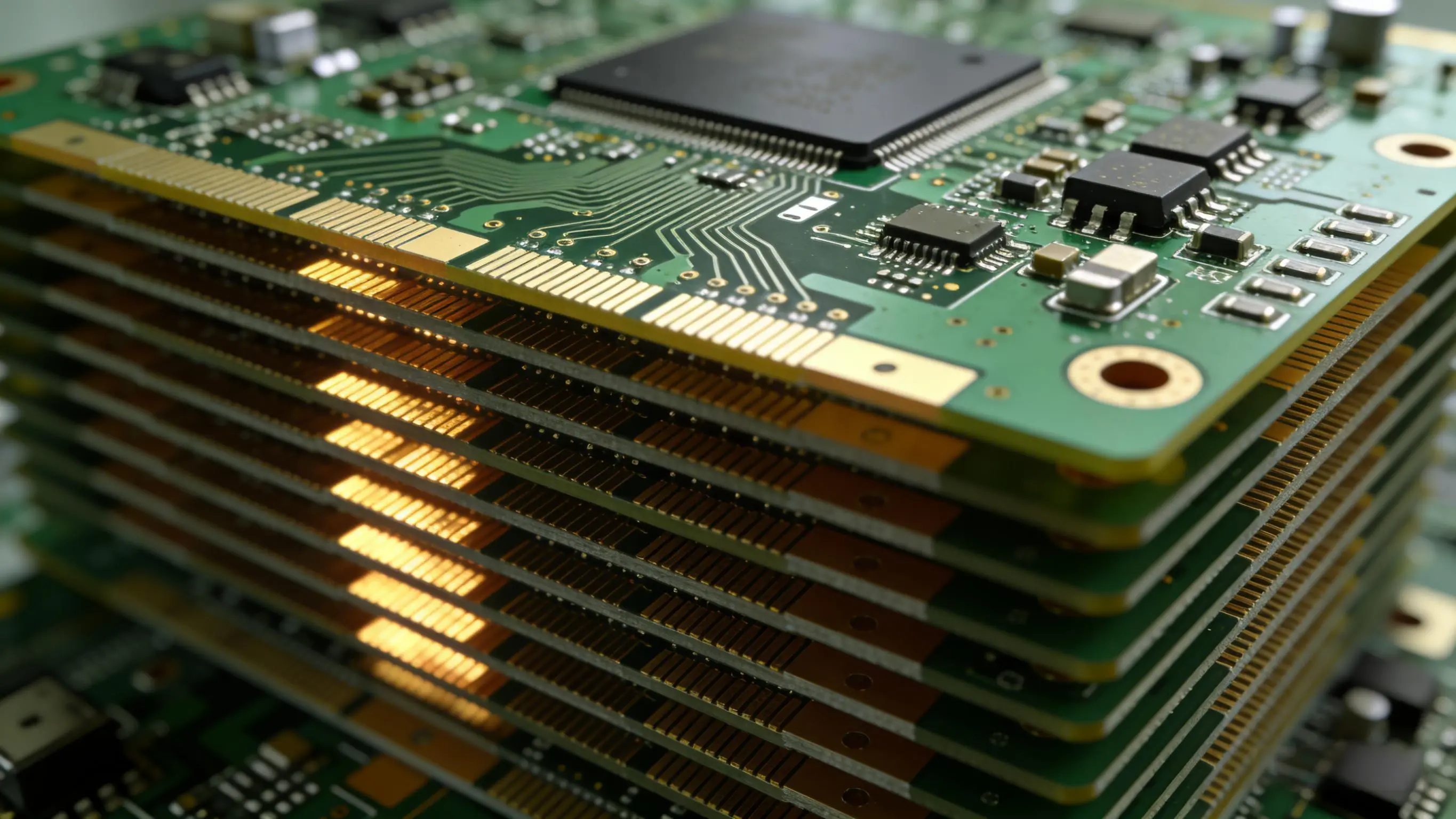
Optical modules integrate laser drivers, transimpedance amplifiers, and clock data recovery chips. Their PCBs typically adopt hybrid stack-ups (high-speed materials such as FR4 combined with ceramic or Rogers materials), with trace widths and spacings down to 50 micrometers, and some pad sizes as small as 0.2 millimeters. Unlike standard PCBAs, the coplanarity error between the optical chip and the electrical chip in an optical module must be controlled within ±15 micrometers; otherwise, coupling efficiency decreases, causing eye diagram closure. Additionally, when operating frequencies exceed 25GHz, any placement offset introduces parasitic inductance and capacitance, degrading high-frequency return loss.
II. Core Process Steps Affecting Placement Accuracy
1. Control Standards for the Solder Paste Printing Process
Solder paste printing is the first step in accuracy control. Optical module PCBAs typically use Type 3 or Type 4 solder paste with particle sizes of 15-25 micrometers. Stencil aperture design should shrink to 80%-90% of the pad area to prevent bridging between adjacent pins. Stencil thickness is recommended at 0.08 millimeters. For BGAs (Ball Grid Arrays) with 0.35mm pitch, nano-coated stencils are required to reduce release resistance. After printing, solder paste thickness variation should be within ±10% of the stencil thickness. 100% inspection using 3D SPI (Solder Paste Inspection) equipment is required, rejecting any solder joints with volume deviation exceeding 15%.
2. Placement Machine Accuracy Classes and Compensation Strategies
Pick-and-place equipment must achieve CPK ≥ 1.33, absolute positioning accuracy of ±20 micrometers, and repeatability of ±10 micrometers. For commonly used CSPs (Chip Scale Packages) and flip chips in optical modules, the placement machine should be equipped with independent upper and lower vision systems. Fiducial marks should use circular or cross patterns with a 1.0mm diameter. PCB expansion and contraction due to temperature require pre-compensation: collect actual Mark point coordinates per panel, calculate scaling factors in software, then correct placement positions. For high-speed channel areas (such as differential pair pads), any manual adjustment beyond automatic compensation is prohibited.
3. Preventing Offset During Reflow Soldering
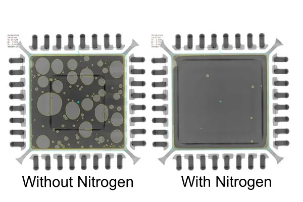
Lead-free reflow soldering has a peak temperature of 245±3℃ and time above liquidus of 60-75 seconds. During hot air convection, for large optical module PCBs (length exceeding 50mm), the temperature difference between corners and center must be controlled within 2℃. Otherwise, the surface tension of molten solder becomes unbalanced, causing component rotation offset. Nitrogen reflow is recommended, with oxygen concentration below 1000ppm, to inhibit solder oxidation while improving wetting symmetry. After reflow, measure component offset using automated optical inspection equipment. Acceptable offset standards: resistors and capacitors within 20% of pad width; QFP (Quad Flat Package) within 15% of lead width; coupling lens areas of optical transceiver subassemblies allow no visible offset.
III. Inspection Methods for Verifying Placement Accuracy
Standard AOI cannot detect buried solder joints or bottom-terminated components within optical modules, requiring the introduction of 3D-X-ray (3D X-ray inspection) systems. For BGA packages, inspect void dimensions: individual voids no larger than 25% of the solder ball diameter, total void volume less than 15% of the solder ball volume. For coplanarity after optical chip placement, use a laser confocal microscope to measure height differences at four corners, requiring overall coplanarity better than 10 micrometers. Keep the first three boards from each production batch for full dimensional measurement, recording coordinate offsets for each optoelectronic device as a reference for material changes or nozzle maintenance.
IV. Common Issues and Countermeasures for High-Precision Placement
In actual production, placement offsets often originate from three factors: insufficient vacuum in the nozzle causing rotational deviation during pickup; uneven oxidation on OSP (Organic Solderability Preservative) finished pads after second-side reflow; and pre-offset of miniature components (0402 and smaller) due to electrostatic attraction during tape feeder indexing. Countermeasures include checking nozzle clogging every 2 hours, completing placement within 4 hours of unpacking OSP boards, and using ionizing fans to eliminate static electricity. If unidirectional offset occurs repeatedly, first investigate periodic errors in the placement machine's X/Y axis glass scale readings rather than directly adjusting coordinates.
With 17 years of expertise in PCBA design, manufacturing, and service, KingshengPCBA is ready to help turn your ideas into reality. Feel free to contact us anytime to discuss your requirements and get a professional quotation.

Please send Email to kspcba@c-alley.com or call us through +86 13828766801 Or submit your inquiry by online form. Please fill out below form and attach your manufacturing files( PCB Gerber files and BOM List) if need quotation. We will contact you shortly.
 +86 13828766801
 kspcba@c-alley.com
 https://www.kingshengpcba.com/
 2/F, Building 6, Tangtou 3rd Industrial Zone, Tangtou Community, Shiyan Town, Baoan District, Shenzhen, China, 518108
We would also like to thank our customers for their trust and support. The company's outstanding achievements are mainly due to the loyalty of our customers, which also encourages and spurs our company to forge ahead.


