* On your first PCB Assembly order!
* Up to $300 discount
 C - A L L E Y
 Home | Events | PCB | About Us | News | Contact Us
During PCBA processing, electrical performance verification and fault diagnosis are the core links of quality control. Embedded test points, as physical probe contact locations reserved during the PCB design phase, provide direct electrical access for subsequent in-circuit testing, functional verification, and debugging. For medium to high complexity PCBA in mass production, the layout and quantity of test points directly affect test coverage, inspection efficiency, and manufacturing cost. The following explains the functional positioning and design rules in two dimensions.
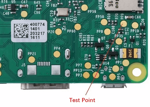
I. Core Functions of Embedded Test Points
1.1 Support for Automated In-Circuit Testing
Embedded test points are the physical interface for ICT equipment probes. ICT sequentially contacts preset test points on the board to measure electrical parameters such as resistance, capacitance, inductance, and diode characteristics, quickly identifying manufacturing defects like shorts, opens, wrong components, and insufficient solder. PCBA without test points cannot achieve fully automated electrical inspection and must rely on manual visual inspection or functional testing, which results in low efficiency and high miss rates.
1.2 Assistance in Functional Debugging and Firmware Programming
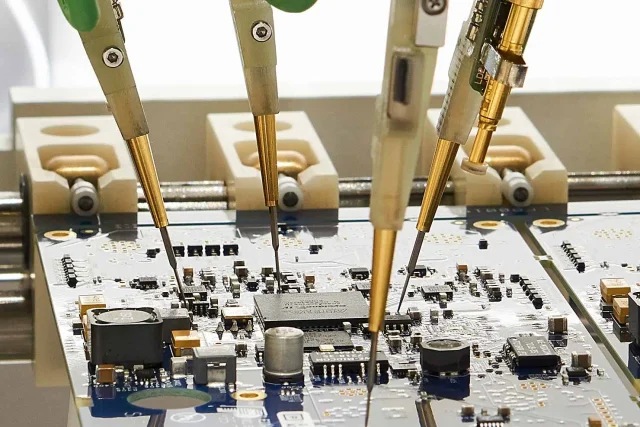
During product development and small-batch production, engineers need to measure critical node waveforms or download programs using oscilloscopes, logic analyzers, or debuggers. Test points provide a stable probe contact location, avoiding direct contact with chip pins that could cause shorts or damage to solder pads. Common debug signals include clock outputs, supply voltages, reset signals, I2C/SPI communication buses, and JTAG/SWD debug interfaces.
1.3 Reduction of Test Fixture Manufacturing Cost
Properly distributed test points allow the use of universal grid needle bed fixtures. When test points are concentrated on a standard pitch grid, the needle bed probes can be arranged according to fixed coordinates, eliminating the need to customize probe positions for each PCBA model. A reduction or disorganized distribution of test points would require a dedicated pneumatic needle bed, increasing the cost of a single fixture.
1.4 Improvement of Test Repeatability and Data Traceability
Fixed test points ensure consistent contact position and pressure for each test, eliminating random errors introduced by manual measurement. The test system can automatically record measurement values from each test point and generate reports for statistical process control and failure analysis.
II. Design Methods for Embedded Test Points
2.1 Test Point Type and Size Specifications
2.2 Electrical Layout Priority Rules
2.3 Physical Layout Constraints
2.4 Design for Manufacturability Checks
III. Cost and Test Coverage Balancing Strategy
High test coverage requires more test points, but test points occupy routing space and increase the number of needle bed probes. In actual design, a tiered strategy is adopted: first-level test points cover all power, ground, and critical control signals, ensuring ICT can detect more than 95% of common manufacturing defects; second-level test points cover debug interfaces and non-critical IOs for use during development and sampling. For high-complexity PCBA with more than 5,000 solder joints, controlling the number of test points between 200 and 300 achieves 90% test coverage without significantly increasing the number of PCB layers.
With 17 years of expertise in PCBA design, manufacturing, and service, Kingsheng PCBA is ready to help turn your ideas into reality. Feel free to contact us anytime to discuss your requirements and get a professional quotation.

Please send Email to kspcba@c-alley.com or call us through +86 13828766801 Or submit your inquiry by online form. Please fill out below form and attach your manufacturing files( PCB Gerber files and BOM List) if need quotation. We will contact you shortly.
 +86 13828766801
 kspcba@c-alley.com
 https://www.kingshengpcba.com/
 2/F, Building 6, Tangtou 3rd Industrial Zone, Tangtou Community, Shiyan Town, Baoan District, Shenzhen, China, 518108
We would also like to thank our customers for their trust and support. The company's outstanding achievements are mainly due to the loyalty of our customers, which also encourages and spurs our company to forge ahead.


