* On your first PCB Assembly order!
* Up to $300 discount
 C - A L L E Y
 Home | Events | PCB | About Us | News | Contact Us
In the PCBA manufacturing process, solder paste printing is the first step of the soldering process. The quality of solder paste printing directly determines the effectiveness of subsequent component placement and reflow soldering. Statistical data indicates that over 60% of soldering defects are related to the solder paste printing process. For PCBA manufacturers, controlling the process parameters of solder paste printing can reduce defect rates at the source and lower rework costs.
I. Key Process Parameters of Solder Paste Printing
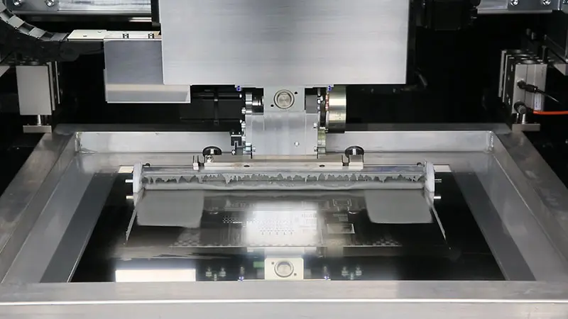
1. Squeegee Pressure and Speed
Insufficient squeegee pressure leads to incomplete solder paste release and insufficient solder volume on pads. Excessive pressure causes the paste to squeeze between pads, creating risks of bridging and short circuits. Recommended squeegee pressure is between 0.5 and 0.8 kilograms per inch of blade length. Squeegee speed is typically controlled between 20 and 40 millimeters per second. Excessive speed results in poor paste rolling and inadequate filling. Excessively slow speed extends the printing cycle and affects production capacity.
2. Separation Speed
The process of separating the stencil from the PCB surface after paste printing is called separation. Separation speed directly affects the shape retention of solder paste on pads. For fine-pitch components (lead pitch below 0.5mm), segmented separation is recommended: first rise slowly at 0.1 to 0.3 millimeters per second for 1 to 2 millimeters, then accelerate to normal speed. This control method reduces paste pulling and tailing.
3. Stencil Aperture Design
The ratio of stencil aperture area to pad area determines paste transfer efficiency. For standard solder mask defined pads, the area ratio (aperture area / wall area) should exceed 0.66. Common stencil thickness ranges from 0.10 to 0.15 millimeters. For 0.4mm pitch QFP components, 0.10mm stencil thickness is recommended, with thinned aperture designs.
II. Common Solder Paste Printing Defects and Countermeasures
1. Insufficient Solder
Insufficient solder appears as inadequate paste coverage or low height on pads. Main causes include stencil clogging, insufficient squeegee pressure, and high paste viscosity. Countermeasures include performing stencil bottom cleaning every 5 to 10 boards. When using an automatic cleaning system, employ a combination mode of wet cleaning, dry cleaning, and vacuum suction. Check whether the paste has been fully reheated, with a minimum reheating time of 2 hours.
2. Bridging
Bridging refers to solder paste connecting between adjacent pads. It is typically caused by excessive squeegee pressure, contaminated stencil bottom, or paste slump. Countermeasures include reducing squeegee pressure and increasing stencil cleaning frequency. Check paste viscosity. The standard viscosity range at room temperature is 800 to 1200 centipoise. Replace with fresh paste when viscosity is too low.
3. Paste Misalignment
Paste not printed accurately at the center of pads and shifts onto the solder mask. Misalignment causes include inaccurate PCB positioning, poor alignment between stencil and PCB, or insufficient stencil tension. Countermeasures include recalibrating the fiducial holes of the positioning fixture. Check stencil tension. Standard tension should exceed 35 Newtons per square centimeter. Replace the stencil when tension falls below 25 Newtons.
III. Quality Monitoring Methods for Solder Paste Printing
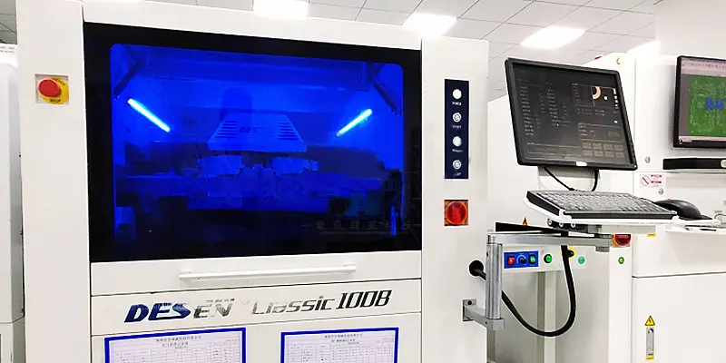
1. Application of SPI Inspection
Solder Paste Inspection (SPI) equipment should be placed after the printer to perform full or sampling inspection. Key parameters monitored by SPI include area, height, volume, and offset. For 01005 and 0201 components, the acceptable height range is 80% to 130% of stencil thickness. The acceptable volume range is 50% to 150% of the target solder paste volume. After setting alarm thresholds, SPI equipment can provide real-time feedback on defect locations and types.
2. Process Capability Index Control
Use Cpk value to measure the stability of the solder paste printing process. The target Cpk value for paste volume is recommended to exceed 1.33. A value above 1.67 indicates excellent process capability. Factories should collect SPI data every 4 hours and plot control charts. When seven consecutive points fall on the same side of the mean, or when points exceed specification limits, immediately stop production to investigate the cause.
3. Stencil Cleaning Cycle Management
Residual paste and flux on the stencil bottom will alter paste thickness in subsequent prints. Automatic cleaning is recommended after every 5 to 10 PCBs. Water-based cleaning agents provide more stable results than alcohol-based cleaners. Perform a manual deep cleaning of the stencil once per week, checking for hardened residue inside mesh apertures.
Conclusion
As the first quality checkpoint in PCBA manufacturing, solder paste printing requires sustained investment from factories in three areas: parameter setting, defect handling, and process monitoring. Establishing standardized work instructions and a regular Cpk analysis system can control solder paste printing defect rates below 1000 ppm.
With 17 years of expertise in PCBA design, manufacturing, and service, KingshengPCBA is ready to help turn your ideas into reality. Feel free to contact us anytime to discuss your requirements and get a professional quotation.

Please send Email to kspcba@c-alley.com or call us through +86 13828766801 Or submit your inquiry by online form. Please fill out below form and attach your manufacturing files( PCB Gerber files and BOM List) if need quotation. We will contact you shortly.
 +86 13828766801
 kspcba@c-alley.com
 https://www.kingshengpcba.com/
 2/F, Building 6, Tangtou 3rd Industrial Zone, Tangtou Community, Shiyan Town, Baoan District, Shenzhen, China, 518108
We would also like to thank our customers for their trust and support. The company's outstanding achievements are mainly due to the loyalty of our customers, which also encourages and spurs our company to forge ahead.


