* On your first PCB Assembly order!
* Up to $300 discount
 C - A L L E Y
 Home | Events | PCB | About Us | News | Contact Us
With the development of electronic products toward miniaturization, high density, and multi-functionality, the market demand for HDI boards continues to grow. HDI boards meet the requirements of products such as smartphones, wearable devices, and medical electronics by incorporating finer circuits, smaller hole diameters, and higher routing densities. In the manufacturing process of HDI boards, drilling is a key technological step. Traditional mechanical drilling suffers from reduced efficiency and severe drill bit wear when the hole diameter falls below 150 microns. The introduction of laser drilling technology has addressed this technical bottleneck. Currently, laser drilling has become the mainstream solution for microvia processing in HDI boards.
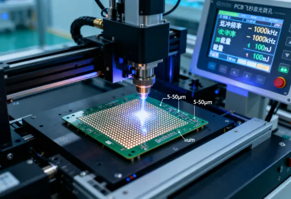
I. Technical Principle and Equipment Types of Laser Drilling
Laser drilling uses a high-energy-density laser beam to irradiate the surface of the board material, causing the material to melt, vaporize, and be removed instantly, forming a microvia. Based on the laser source, there are three main types: ultraviolet laser, carbon dioxide laser, and solid-state laser. Ultraviolet lasers have a short wavelength and a small focused spot, making them suitable for direct processing of copper layers and resins. Carbon dioxide lasers have a high absorption rate for organic resin materials and are commonly used to remove resin and glass fiber layers. In HDI board manufacturing, a combination of ultraviolet and carbon dioxide lasers is often used to complete copper foil window opening and dielectric layer via formation, respectively.
II. Core Advantages of Laser Drilling in HDI Boards
(A) Achieving Microvia Diameters
Laser drilling can stably process microvias with diameters ranging from 50 microns to 100 microns, with a minimum achievable diameter of 25 microns. This is far below the conventional lower limit of 150 microns for mechanical drilling. For the micro-vias, buried vias, and blind vias required by HDI boards, laser drilling provides precise control over via diameters, meeting the demanding requirements for via spacing and routing space in high-density interconnect designs.
(B) Improving Drilling Positioning Accuracy
Laser drilling employs a CNC scanning system, achieving repeated positioning accuracy within ±5 microns. Mechanical drilling suffers from drill bit deviation and spindle runout, with positioning errors typically around ±25 microns. For densely arranged microvia arrays on HDI boards, laser drilling ensures accurate alignment of vias with underlying pads, reducing the risk of electrical connection failure caused by eccentricity.
(C) Reducing Material Damage During Drilling
Mechanical drilling, with its high-speed rotation, exerts significant axial force and cutting stress on the board material, easily causing resin cracks, copper foil lifting, and inner layer separation. Laser drilling is a non-contact process with no cutting force, and the heat-affected zone is controlled within a range of 10 to 20 microns. By optimizing pulse width and energy density, carbonization of the via wall and micro-cracks can be significantly reduced, leading to improved via wall quality.
(D) Improving Stacked-Layer Drilling Efficiency for Multilayer Boards
HDI boards often contain multiple build-up layers, such as second-order and third-order blind vias. Laser drilling can penetrate a single dielectric layer in one pass without the need for tool changes or re-alignment. For high-density boards requiring the processing of thousands of microvias, the scanning speed of laser drilling can reach hundreds of holes per second, resulting in a processing cycle that is much shorter than the step-by-step approach of mechanical drilling.
III. Key Control Parameters in the Laser Drilling Process
(A) Laser Power and Pulse Width
Different thicknesses of copper foil and dielectric layers require corresponding laser power levels. During the copper window opening stage, insufficient power fails to penetrate the copper layer, while excessive power can over-etch the inner layer pad. Pulse width is typically controlled within the range of 10 to 100 nanoseconds. Shorter pulse widths are beneficial for reducing thermal diffusion.
(B) Number of Passes and Cleaning Process
A single laser pulse is often insufficient to form a smooth via bottom. In production, multiple scans are employed. Low energy is used first to remove most of the material, followed by higher energy to refine the via shape. After processing, a desmearing process is necessary to remove residual carbonized material from the via wall, ensuring good adhesion for subsequent copper plating.
(C) Material-Specific Parameters
Different resin systems exhibit varying absorption rates for laser energy. Standard FR-4 material can be processed using a carbon dioxide laser. However, for high-frequency materials containing ceramic fillers or high glass transition temperature resins, an ultraviolet laser or higher laser energy density is required.
IV. Practical Considerations in Application
The via wall shape produced by laser drilling is an inverted funnel, with the opening diameter larger than the bottom diameter. This requires sufficient pad dimensions to reserved during the design phase. For dielectric layers exceeding 100 microns in thickness, a single laser pass is insufficient to form the via directly, requiring a hybrid process of pre-drilling followed by etching. Furthermore, different batches of copper-clad laminate material may exhibit variations in resin uniformity, requiring parameter verification before production.
With 17 years of expertise in PCBA design, manufacturing, and service, KingshengPCBA is ready to help turn your ideas into reality. Feel free to contact us anytime to discuss your requirements and get a professional quotation.

Please send Email to kspcba@c-alley.com or call us through +86 13828766801 Or submit your inquiry by online form. Please fill out below form and attach your manufacturing files( PCB Gerber files and BOM List) if need quotation. We will contact you shortly.
 +86 13828766801
 kspcba@c-alley.com
 https://www.kingshengpcba.com/
 2/F, Building 6, Tangtou 3rd Industrial Zone, Tangtou Community, Shiyan Town, Baoan District, Shenzhen, China, 518108
We would also like to thank our customers for their trust and support. The company's outstanding achievements are mainly due to the loyalty of our customers, which also encourages and spurs our company to forge ahead.


