* On your first PCB Assembly order!
* Up to $300 discount
 C - A L L E Y
 Home | Events | PCB | About Us | News | Contact Us
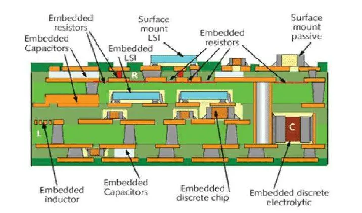
As electronic products evolve toward miniaturization, higher frequencies, and higher interconnection densities, traditional surface-mounted resistors and capacitors on PCBs can no longer meet the demands of high-end equipment regarding space utilization and signal integrity. Buried resistor and buried capacitor technology addresses this by fabricating resistive and capacitive components directly into the inner layers of the PCB. This reduces the number of surface-mounted devices, shortens signal paths, and has become a critical process in high-end communications, medical equipment, military, and aerospace applications. This blog introduces the basic principles, material selection, design considerations, and process control methods of this technology.
1. Basic Principles of Buried Resistor and Buried Capacitor Technology
1.1 Buried Resistor Technology
A buried resistor refers to a planar resistive material embedded in the inner layer of a PCB. Target resistance is achieved by controlling the thickness, length, and width of the resistive material. Common buried resistor materials include resistive foils (e.g., Ohmega-Ply) and thick-film resistor pastes. The resistive foil is laminated onto the substrate, and the resistor pattern is formed by photolithography and etching. The resistor paste is applied by screen printing and then sintered and cured.
1.2 Buried Capacitor Technology
Buried capacitors utilize distributed capacitance between inner layer planes to form an energy storage structure. A typical buried capacitor structure consists of a thin dielectric layer (25μm to 100μm thick) between the power and ground planes. The material is a high-dielectric-constant resin or ceramic-filled composite. Double-sided copper-clad laminates are etched to form capacitor plates, and the interlayer capacitance replaces discrete decoupling capacitors.
2. Material Selection and Key Parameters
2.1 Buried Resistor Material Parameters
The mainstream buried resistor material is a nickel-phosphorus alloy resistive foil with a sheet resistance ranging from 25Ω/□ to 250Ω/□. Sheet resistance indicates the resistance value per square of material. The resistance is calculated based on the length-to-width ratio of the resistor pattern. Thickness tolerance is controlled within ±5% to ensure resistance accuracy. The temperature coefficient is below 100ppm/℃, suitable for operating temperatures from -55℃ to 125℃.
2.2 Buried Capacitor Material Parameters
Dielectric materials are epoxy or polyimide composites with a Dk value between 10 and 30. Typical dielectric thickness is 50μm, providing a capacitance density of 0.5nF/cm² to 5nF/cm². The breakdown voltage must exceed 500V. The dissipation factor is less than 0.02 at 1MHz, meeting the signal integrity requirements for high frequencies.
3. Design Methods and Process Considerations
3.1 Buried Resistor Design Method
Determine the target resistance and power of each buried resistor. Set the resistor length between 0.5mm and 2mm. Calculate the width using the formula: Resistance = Sheet Resistance × (Length / Width). Keep power density below 0.1W/mm². Multiple buried resistors can be connected in series or parallel, but patterns cannot cross within the same plane. Design software must include buried resistor layer definition and resistance value verification rules.
3.2 Buried Capacitor Design Method
Calculate the total capacitance required between the power and ground planes. Divide the target capacitance by the capacitance per unit area to obtain the required area. Multiple power domains correspond to multiple buried capacitor units. Isolation rings are placed between units to prevent short circuits. Maintain a minimum distance of 5mm between the buried capacitor area and the board edge to avoid capacitance drift caused by resin flow during lamination.
3.3 Process Control
Buried resistor fabrication uses a subtractive method: start with a substrate laminated with resistive foil → apply photoresist → expose and develop → etch away excess resistive material → strip the photoresist. Etching time must be precisely controlled; over-etching can increase resistance by 5%-15%. For buried capacitors, after etching the top and bottom plate patterns, the dielectric layer is fully filled between the plates during high-temperature lamination. Lamination temperature: 180℃-200℃, pressure: 300psi-400psi, duration: 60 minutes. Use four-wire Kelvin testing for buried resistor resistance measurement. Use an LCR meter at 1kHz for capacitance measurement.
4. Typical Application Scenarios
4.1 High-Speed Digital Communication Equipment
In optical modules and backplanes, buried capacitors reduce power-ground impedance and lower simultaneous switching noise in the 10MHz to 1GHz range. Buried resistors are used for signal termination matching, reducing stub length and improving eye diagram quality.
4.2 Medical Implantable Devices
Cardiac pacemakers and neurostimulators use buried resistors and capacitors to reduce the number of solder joints and improve long-term reliability. Buried resistors form precision voltage divider networks with resistance drift below 0.1% per year.
4.3 RF and Microwave Modules
Buried resistors and capacitors eliminate parasitic inductance from surface-mounted components, allowing antenna matching networks to maintain stable response above 6GHz. Buried capacitors serve as isolation capacitors between DC bias and RF ground, with equivalent series inductance below 200pH.
Conclusion
Buried resistor and buried capacitor technology integrates passive components inside the PCB, resolving the conflict between integration density and high-frequency performance in high-end applications. Material selection must match resistance/capacitance density and temperature characteristics. Design requires optimizing pattern geometry and electrical parameters. Manufacturing demands specialized etching and lamination control.
With 17 years of expertise in PCBA design, manufacturing, and service, KingshengPCBA is ready to help turn your ideas into reality. Feel free to contact us anytime to discuss your requirements and get a professional quotation.

Please send Email to kspcba@c-alley.com or call us through +86 13828766801 Or submit your inquiry by online form. Please fill out below form and attach your manufacturing files( PCB Gerber files and BOM List) if need quotation. We will contact you shortly.
 +86 13828766801
 kspcba@c-alley.com
 https://www.kingshengpcba.com/
 2/F, Building 6, Tangtou 3rd Industrial Zone, Tangtou Community, Shiyan Town, Baoan District, Shenzhen, China, 518108
We would also like to thank our customers for their trust and support. The company's outstanding achievements are mainly due to the loyalty of our customers, which also encourages and spurs our company to forge ahead.


