* On your first PCB Assembly order!
* Up to $300 discount
 C - A L L E Y
 Home | Events | PCB | About Us | News | Contact Us
In the PCBA manufacturing process, the flatness of the PCB substrate is a key factor affecting SMT assembly quality. With the trend toward miniaturization and high density in electronic components, SMT placement has increasingly stringent requirements for PCB coplanarity. PCB warpage refers to the non-uniform deformation of the substrate under thermal stress, mechanical stress, or internal material stress, causing the board surface to deviate from the ideal plane. This article analyzes the causes of PCB warpage from three dimensions—material, design, and process—and describes its typical impact on SMT assembly.
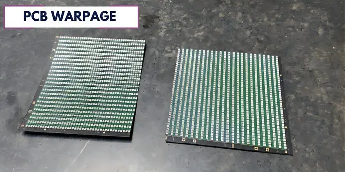
I. Main Causes of PCB Warpage
1. Material Factors
Non-uniform coefficient of thermal expansion (CTE) of the PCB base material is a root cause of warpage. The CTE difference between copper foil and resin substrate in different layers is significant. When temperature changes, the inconsistent expansion and contraction of each layer generate internal stress. A glass transition temperature (Tg) that is too low or incomplete curing of prepreg (PP) materials can also cause dimensional changes during subsequent heating. Additionally, mixing PP materials from different suppliers can lead to mismatched shrinkage rates after lamination.
2. Design Factors
Asymmetric layer stack-up is the most common warpage trigger on the design side. For example, an odd number of layers or uneven copper thickness distribution across layers causes unbalanced stress on the top and bottom surfaces of the board. The difference in heat capacity between large copper areas and open areas amplifies thermal deformation during reflow soldering. Dense via placement in a local area can also reduce structural stiffness there.
3. Process Factors
Excessively fast ramp rates or uneven pressure during the lamination process can result in incomplete resin flow and residual curing stress. If PCBs are stored without being pressed flat or absorb moisture, rapid vaporization of that moisture during the SMT preheat stage creates expansion stress. Improper V-cut depth or excessively thin remaining connection points in panelization can cause warpage even before depaneling.
II. Specific Impact of PCB Warpage on SMT Assembly
1. Affects Solder Paste Printing Accuracy
A warped board prevents the stencil from maintaining coplanar contact with the PCB. When the board center bows upward, the gap between the stencil and PCB edges increases, causing solder paste squeeze-out and bridging. When the board center sags downward, excessive pressure in the center area squeezes paste outside the pad area, risking short circuits. For fine-pitch components (e.g., 0.4mm pitch QFN), warpage-induced printing offset can directly lead to mass open circuits.
2. Causes Placement Shift and Tombstoning
When the pick-and-place nozzle picks and positions components, the placement machine assumes the PCB is flat. If local warpage exists at the placement location, the actual component landing position will deviate from the pad center. For small passive components (e.g., 0402, 0201), off-center placement leads to unbalanced wetting forces of molten solder during reflow, easily causing tombstoning, drawbridging, or one end lifting off the pad.
3. Induces Reflow Soldering Defects
During the high-temperature zone of reflow (approximately 240-260°C), PCB warpage changes dynamically. Height differences between adjacent solder pads caused by warpage create gaps or lifting between component leads and pads, resulting in insufficient solder, cold joints, or open circuits. For bottom-terminated packages such as BGA and LGA, warpage prevents some solder balls from simultaneously contacting both the pad and the package bottom. After the solder balls melt, open circuits or shorts occur. Severe warpage can also cause component body cracking due to tensile stress during cooling.
4. Reduces Assembly Yield and Reliability
As a single PCB is repeatedly heated across multiple SMT processes, warpage can progressively worsen. Warped boards cannot make good contact with test probes in test fixtures, causing false failures. During final assembly at the customer site, warpage can prevent screws from tightening properly or cause interference with the enclosure. Over long-term use, residual stress may induce solder joint fatigue cracks.
III. Suggested Control Directions
Before production, use warpage measurement tools (such as a granite surface plate with feeler gauges or laser distance measurement) for incoming PCB sampling inspection. The typical acceptance standard is within 0.5%–0.75% of the diagonal length. On the SMT line, optimize the reflow soldering profile by lowering the peak temperature and extending the soak zone time to release internal stress. Using carriers (trays or magnetic clamps) to physically press flat warped boards is a short-term mitigation measure. The fundamental solution remains controlling the PCB supplier's lamination process specifications and ensuring symmetric stack-up design.
Controlling PCB warpage not only improves SMT first-pass yield but also serves as a prerequisite for long-term reliability of electronic products. As an independent website operator, you can use the technical content above to demonstrate professional inspection and process optimization capabilities to customers.
With 17 years of expertise in PCBA design, manufacturing, and service, KingshengPCBA is ready to help turn your ideas into reality. Feel free to contact us anytime to discuss your requirements and get a professional quotation.

Please send Email to kspcba@c-alley.com or call us through +86 13828766801 Or submit your inquiry by online form. Please fill out below form and attach your manufacturing files( PCB Gerber files and BOM List) if need quotation. We will contact you shortly.
 +86 13828766801
 kspcba@c-alley.com
 https://www.kingshengpcba.com/
 2/F, Building 6, Tangtou 3rd Industrial Zone, Tangtou Community, Shiyan Town, Baoan District, Shenzhen, China, 518108
We would also like to thank our customers for their trust and support. The company's outstanding achievements are mainly due to the loyalty of our customers, which also encourages and spurs our company to forge ahead.


