* On your first PCB Assembly order!
* Up to $300 discount
 C - A L L E Y
 Home | Events | PCB | About Us | News | Contact Us
I.Now that fibre-optic broadband has become widely available, the optical network terminal (ONT), as an essential piece of equipment for operators’ in-home installations, plays a crucial role in converting optical signals to electrical signals, distributing the network, routing traffic and providing dial-up internet access. The PCBA circuit board is the heart and nervous system of the ONT, determining the stability of broadband speeds, the accuracy of signal conversion, network latency and the device’s service life. It can be said that the overall performance of an ONT essentially depends on the design, material selection, manufacturing processes and reliability standards of its internal PCBA.
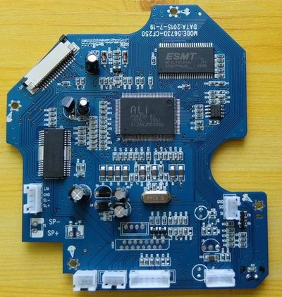
III.The ONT PCBA integrates core components such as optical module chips, main control chips, switching circuits, power management units, memory chips, Ethernet port drivers and Wi-Fi RF circuits. Its primary function is to convert the optical signals transmitted via the operator’s fibre optic cable into digital electrical signals, which are then distributed to end devices such as routers, computers, televisions and smart home devices. It also performs functions such as broadband dialling, LAN forwarding and wireless WiFi transmission, making it an indispensable and critical component in the entire home network infrastructure.
III.Compared to ordinary electronic products, optical network terminals operate 24 hours a day, year-round, placing extremely high demands on the PCBA’s heat resistance, resistance to ageing and stability. Substandard PCBA boards are prone to issues such as network disconnections, sluggish internet speeds, skyrocketing latency, overheating and system crashes, and weak WiFi signals, which directly impact the normal use of home office setups, online classes, high-definition video streaming and whole-home smart devices. Consequently, genuine optical modem PCBA boards generally utilise high-TG heat-resistant boards, which are resistant to high voltage and less prone to moisture-induced deformation, making them suitable for long-term, uninterrupted operation under continuous load.
IV.At the circuit design level, ONT PCBA places great emphasis on electromagnetic compatibility and signal isolation. Optical-to-electrical conversion involves precision low-signal processing and is highly susceptible to power fluctuations and radio-frequency interference. The design employs a zoned layout for digital, analogue and RF circuits, with separate routing for high- and low-voltage signals and independent layer shielding. This effectively suppresses electromagnetic crosstalk, ensuring the sensitivity of optical signal reception and the accuracy of data transmission. For Gigabit and 10 Gigabit ONT PCBs, precise impedance control and differential equal-length routing are also implemented to ensure stable, packet-loss-free performance for Gigabit broadband and IPTV HD services.
V.In terms of manufacturing processes, high-quality ONT PCBs utilise high-precision SMT assembly techniques, ensuring the accurate placement of micro-components and uniform, full solder joints, thereby eliminating the risk of cold or missing solder joints. The power supply circuitry incorporates voltage regulation, filtering, and overcurrent and overvoltage protection designs to prevent chips from being damaged by mains voltage fluctuations. Some operator-customised optical modems also undergo a triple-proof coating treatment to provide dust and moisture resistance, enabling them to withstand the confined, hot and poorly ventilated installation environments of low-voltage cabinets, thereby delaying circuit ageing.
VI.With the widespread adoption of gigabit broadband, whole-home fibre networks and FTTR fibre networking, the new generation of optical modems is evolving towards 10-gigabit uplink speeds, dual-band Wi-Fi, multi-port concurrency and intelligent operation and maintenance. This places higher demands on the PCBA’s integration, high-frequency performance and heat dissipation capabilities. High-density integration, miniaturised layouts and low-loss signal design have become the industry standard.
In summary, whilst optical modems may appear small and unremarkable, the PCBA inside serves as the core hardware supporting broadband communication links. Only through high-quality circuit design, reliable PCB materials and components, and mature SMT processes can optical modems operate stably over the long term, ensuring a high-speed, low-latency, and uninterrupted network experience for households and businesses.
With 17 years of expertise in PCBA design, manufacturing, and service, KingshengPCBA is ready to help turn your ideas into reality. Feel free to contact us anytime to discuss your requirements and get a professional quotation.

Please send Email to kspcba@c-alley.com or call us through +86 13828766801 Or submit your inquiry by online form. Please fill out below form and attach your manufacturing files( PCB Gerber files and BOM List) if need quotation. We will contact you shortly.
 +86 13828766801
 kspcba@c-alley.com
 https://www.kingshengpcba.com/
 2/F, Building 6, Tangtou 3rd Industrial Zone, Tangtou Community, Shiyan Town, Baoan District, Shenzhen, China, 518108
We would also like to thank our customers for their trust and support. The company's outstanding achievements are mainly due to the loyalty of our customers, which also encourages and spurs our company to forge ahead.


