* On your first PCB Assembly order!
* Up to $300 discount
 C - A L L E Y
 Home | Events | PCB | About Us | News | Contact Us
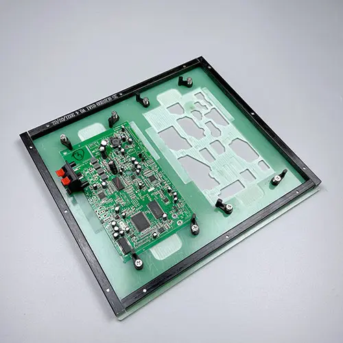
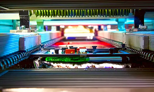
In PCBA processing, wave soldering is a core process for through-hole component soldering. As the fixture that carries the PCB through the soldering machine, the pallet’s design directly affects soldering quality, production efficiency, and yield. This article analyzes its specific impact on soldering quality from three dimensions: pallet material, opening method, and support structure.
I. Relationship Between Pallet Material Selection and Soldering Defects
1.1 Thermal Conductivity Differences Between Composite and Metal Materials
Common pallet materials include fiberglass composites and synthetic stone. Fiberglass composites have low thermal conductivity and absorb little heat, resulting in small temperature fluctuations at PCB pad areas during soldering, making them suitable for precision boards. Metal pallets conduct heat quickly, easily causing localized temperature drops on the PCB, reducing solder fluidity and leading to bridging or cold solder joints.
1.2 Effect of Material Thickness on Thermal Compensation
Pallet thickness is typically controlled between 3 and 6 mm. Excessive thickness absorbs too much heat, causing abnormal cooling rates at solder joints and forming micro-cracks. Insufficient thickness leads to inadequate rigidity, causing the PCB to vibrate under wave impact, resulting in poor wetting.
II. Parametric Control of Pallet Opening Design
2.1 Geometric Relationship Between Opening Size and Solder Joint Formation
The pallet opening diameter should be 1.5 to 2 times the pad diameter. If the opening is too small, solder surface tension blocks filling inside the opening, causing insufficient through-hole solder rise. If too large, solder leaks from the component side, forming solder balls on the bottom side. For components with pin pitch less than 2 mm, a flow channel structure is recommended, with elongated holes along the pin arrangement direction to improve solder flow path.
2.2 Failure Modes of Clearance Areas
The pallet must provide clearance for already assembled SMT components. Insufficient clearance depth causes the pallet to press on SMT solder joints, leading to joint cracking or component shifting. A minimum clearance of 0.5 mm should be maintained between the clearance edge and the SMT component body. The clearance sidewall angle should exceed 15 degrees to avoid solder wicking up onto the pallet.
III. Mechanical Influence of Pallet Support Structures
3.1 Support Point Layout and PCB Warpage Suppression
Large or flexible PCBs tend to bend during wave soldering due to high temperature and wave impact. When the height deviation of pallet support pins exceeds 0.1 mm, the distance between the PCB and the wave nozzle becomes inconsistent, resulting in solder joint height variation beyond standard. Support points should be placed under high-stress areas of the PCB, such as connectors and transformers. High-temperature silicone pads added to the top of support pins compensate for PCB thickness tolerance.
3.2 Hold-Down Devices and Floating Control
The pallet is equipped with elastic hold-down pins or magnetic clamps to keep the PCB flat against the pallet surface. When hold-down force exceeds 2 Newtons, component bodies may shift under pressure. When force is below 0.5 Newtons, the PCB may float, causing pins to detach from the solder wave. Hold-down pin density should be at least 3 per 100 cm².
IV. Process Validation Methods for Pallet Design
4.1 Thermal Imaging Inspection
The first-article pallet is run through the soldering machine without solder, using a thermal imager to measure temperature distribution on the PCB surface. A temperature difference exceeding 10°C across the same PCB indicates uneven heat absorption or improper opening design.
4.2 Dye Penetration Test
The post-soldering PCBA is soaked in red penetrant dye, then cleaned and inspected for dye staining on solder joints. Dye lines appearing at solder joints under pallet support areas indicate support-induced micro-cracks. Dye staining at the root of pins on the component side indicates insufficient through-hole solder rise, requiring larger pallet openings.
4.3 Lifecycle Management
After 5,000 soldering cycles, pallet opening wear is measured. Pallets with wear exceeding 0.2 mm are scrapped and replaced. Each pallet is assigned an ID and its usage count is recorded, with a regular maintenance schedule established.
Conclusion
Wave soldering pallet design serves as the physical interface connecting process parameters and soldering quality. Quantified design focusing on thermal uniformity of materials, geometric precision of openings, and mechanical balance of support can systematically reduce defects such as bridging, cold joints, and insufficient through-hole rise. It is recommended that PCBA factories review pallet design specifications quarterly and establish a pallet design knowledge base tailored to specific product types.
With 17 years of expertise in PCBA manufacturing, and service, Kingsheng PCBA is ready to help turn your ideas into reality. Feel free to contact us anytime to discuss your requirements and get a professional quotation.

Please send Email to kspcba@c-alley.com or call us through +86 13828766801 Or submit your inquiry by online form. Please fill out below form and attach your manufacturing files( PCB Gerber files and BOM List) if need quotation. We will contact you shortly.
 +86 13828766801
 kspcba@c-alley.com
 https://www.kingshengpcba.com/
 2/F, Building 6, Tangtou 3rd Industrial Zone, Tangtou Community, Shiyan Town, Baoan District, Shenzhen, China, 518108
We would also like to thank our customers for their trust and support. The company's outstanding achievements are mainly due to the loyalty of our customers, which also encourages and spurs our company to forge ahead.


