* On your first PCB Assembly order!
* Up to $300 discount
 C - A L L E Y
 Home | Events | PCB | About Us | News | Contact Us
While many companies perceive PCB design as simply "drawing boards," it is fundamentally a systems engineering endeavor involving circuit design, mechanical integration, signal integrity, and manufacturing processes. Below is a breakdown of engineers’ core tasks by project phase:
I. Requirements Analysis & System Definition (Determines 80% of Success)
Engineers start by defining the problem, not drawing the board:
① Functional decomposition: Power delivery, communication interfaces, control logic.
② Component selection: MCUs, ICs, power chips (considering availability/alternates).
③ Cost & supply chain evaluation: Scalability for mass production.
④ PCB layer stackup planning: 2/4/6+ layers based on complexity.
Impact: Cost, performance, and manufacturability (DFM).
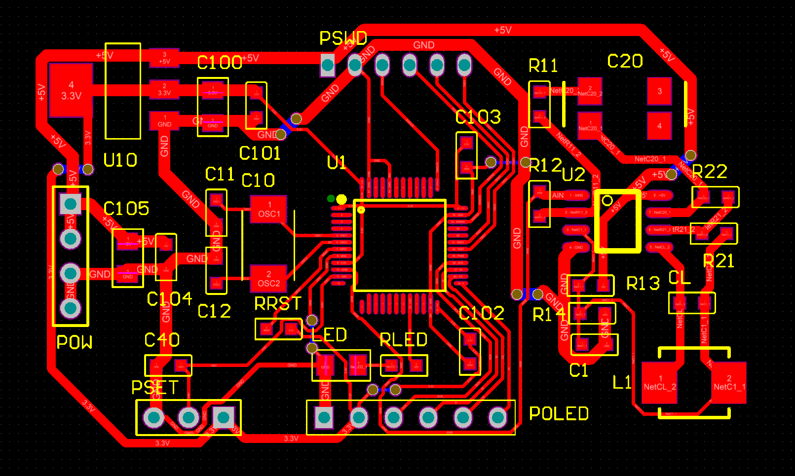
II. Schematic Design (Electrical Logic Core)
Beyond wiring, schematics reflect engineering rigor:
① Power integrity: Decoupling, PDN (Power Distribution Network).
② Signal interfaces: SPI/I2C/USB/high-speed protocols.
③ Footprint validation: Avoiding package mismatches.
④ ERC checks (Electrical Rule Check).
Common pitfalls: Poor power filtering → instability; missing interface protection → field failures.
III. PCB Library Management (Root of Many Issues)
Critical tasks:
① Footprint design: Pad dimensions, spacing, solder mask.
② 3D model integration: Mechanical interference checks.
③ BGA-specific rules: Fanout strategies, via placement. Industry truth: Footprint errors = 100% rework.
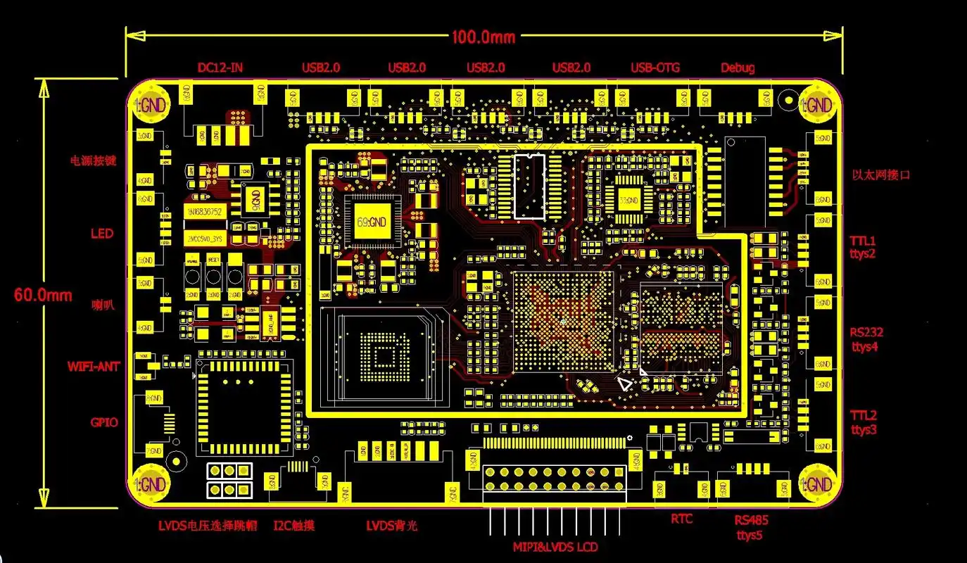
IV. Component Placement (Dictates 70% of Performance)
Key considerations:
① Functional zoning: Power/analog/digital isolation.
② Signal path optimization: Minimal routing length.
③ Thermal management: High-power component placement.
④ High-speed devices: DDR, USB, RF positioning. IPC-2221 standards: Prioritize power/ground, high-frequency signals, and analog-digital separation.
V. PCB Routing (High-Skill Phase)
Low-speed design:
① Trace width/spacing, return path continuity. High-speed design:
② Impedance control (50Ω/90Ω differential). ③ Length matching, differential pair routing.
Theories applied: Signal Integrity (SI), Power Integrity (PI).
VI. EMC/EMI Optimization (Certification Critical)
Failures here often require costly fixes:
① Return path design, ground plane integrity.
② Filtering/shielding strategies (single-point vs. multi-point grounding).
VII. DFM/DFA Review (Manufacturability Analysis)
Pre-fabrication checks:
① Minimum trace/clearance, via types (blind/buried/through-hole).
② Solder pad design, panelization. Standards: IPC-A-600 (quality), IPC-7351 (footprints).
VIII. Prototyping
① Small-batch PCB fabrication.
② SMT assembly.
③ Initial functional tests.
IX. Testing & Validation
① Functional debugging.
② Signal testing (oscilloscope/spectrum analyzer).
③ EMC compliance fixes.
④ Environmental reliability tests. Reality: 70%+ issues originate in design.
X: Key Takeaway
A successful PCB project is not "done at layout"—it’s a systemic process spanning design, fabrication, and validation. Every dollar saved in design may cost 10x–100x in post-production fixes. For professional PCB design, prototyping, and PCBA services, choosing a full-capability team with engineering expertise outweighs "low-cost" options.
With 17 years of expertise in PCBA design, manufacturing, and service, KingshengPCBA is ready to help turn your ideas into reality. Feel free to contact us anytime to discuss your requirements and get a professional quotation.

Please send Email to kspcba@c-alley.com or call us through +86 13828766801 Or submit your inquiry by online form. Please fill out below form and attach your manufacturing files( PCB Gerber files and BOM List) if need quotation. We will contact you shortly.
 +86 13828766801
 kspcba@c-alley.com
 https://www.kingshengpcba.com/
 2/F, Building 6, Tangtou 3rd Industrial Zone, Tangtou Community, Shiyan Town, Baoan District, Shenzhen, China, 518108
We would also like to thank our customers for their trust and support. The company's outstanding achievements are mainly due to the loyalty of our customers, which also encourages and spurs our company to forge ahead.


