* On your first PCB Assembly order!
* Up to $300 discount
 C - A L L E Y
 Home | Events | PCB | About Us | News | Contact Us
High-power components face significant thermal management challenges during PCBA soldering, including thermal stress, solder joint cracks, and package delamination. This article systematically addresses the formation mechanisms of thermal management issues and provides specific measures for reflow profile optimization, localized supplemental heating, solder paste selection, thermal via layout, and rework control.
I. Formation Mechanism of Thermal Management Issues
1.1 Thermal Characteristics of High-Power Components
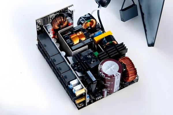
High-power components in PCBA processing exhibit high heat generation per unit area and large local temperature gradients. Typical components include MOSFETs, IGBTs, power diodes, and DC-DC converter modules. During soldering, these components must withstand the thermal shock of reflow or wave soldering, while their internal structures are sensitive to localized overheating.
1.2 Pathways for Generating Thermal Stress During Soldering
Thermal stress during soldering arises from three sources. First, the difference in coefficient of thermal expansion between components and the PCB substrate. Second, transient temperature differences between soldered and non-soldered areas. Third, mechanical constraints caused by solder solidification and shrinkage during the cooling phase. When local temperatures exceed the component's rated tolerance, delamination may occur at the interface between the internal die and the packaging material.
1.3 Typical Failure Mode Statistics
Industry data shows that among soldering-related failures of high-power components, solder joint cracks account for approximately 42%, internal bond wire detachment accounts for 28%, substrate delamination accounts for 18%, and the remainder consists of lead breakage and package cracking. All of these failures are directly related to inadequate thermal management measures.
II. Control of Key Process Parameters
2.1 Reflow Soldering Temperature Profile Adjustment
For high-power components, a segmented ramp-up profile is recommended. The preheat stage ramp rate is controlled at 1.0 to 1.5°C per second, with the preheat endpoint temperature set to 150 to 170°C. The soak stage duration is extended to 90 to 120 seconds to ensure temperature uniformity between the PCB and components. The peak temperature at the reflow stage is lowered by 5 to 8°C, adjusted downward to 235 to 240°C compared to standard processes. The cooling stage ramp rate is controlled at 2 to 4°C per second to avoid excessive stress from rapid cooling.
2.2 Application of Localized Supplemental Heating
When a PCB contains both high-power components and large heat-absorbing components, bottom-side auxiliary heating or infrared localized heating can be used. The bottom heater temperature is set to 100 to 120°C to raise the overall substrate temperature. This method reduces the actual temperature difference at high-power component solder joints from 15°C to within 5°C.
2.3 Solder Paste Selection and Stencil Design
Select SAC305-series solder paste with silver content of 3.8% to 4.2%, which offers better thermal fatigue resistance than low-silver alloys. The stencil aperture area ratio must exceed 0.66. For thermal pads, an array of apertures is recommended, with an aperture ratio of 50% to 70%. Individual aperture dimensions are 1.2 to 1.5 mm square, with a pitch of 0.3 to 0.4 mm.
III. Thermal Management Interventions at the Design Stage
3.1 Thermal Via Layout Specifications
Thermal vias should be placed under the bottom thermal pad of high-power components. Recommended via diameter is 0.3 to 0.4 mm, with a pitch of 1.0 to 1.2 mm. The via walls require copper plating with a minimum thickness of 20 µm. The back side of the vias can be connected to a ground copper plane or a dedicated heat dissipation layer.
3.2 Copper Pour and Solder Mask Treatment
The width of the copper pour connected to the pads of a power component shall be no less than 1.5 times the width of the component lead. The solder mask opening for the thermal pad shall extend at least 0.5 mm beyond each edge of the pad to allow adequate solder filling. Avoid placing large, unsegmented copper areas near the pads to reduce the heat-sink effect.
3.3 Thermal Balancing Structures
When multiple high-power components are placed in the same area of the PCB, thermal isolation channels with a minimum width of 2 mm shall be reserved between components. The inner-layer copper within the area projected under the back side of the power component shall be kept continuous, with thermal vias arrays to achieve thermal continuity between layers.
IV. Inspection and Reliability Qualification
4.1 Post-Soldering Thermal Inspection Methods
Use a thermal imaging camera to measure the case temperature of the component under powered operation. The test environment temperature is 25°C, and the component is loaded to 80% of its rated power. The acceptance criterion is that the measured temperature deviates from the design simulation value by no more than 10°C. Additionally, measure the temperature difference between adjacent components. A difference greater than 15°C indicates a poor thermal design.
4.2 Accelerated Thermal Cycling Test
Perform temperature cycling tests in accordance with IPC-9701. Low temperature of -40°C for 15 minutes, high temperature of 125°C for 15 minutes, with a transition time not exceeding one minute. After 500 cycles, a solder joint resistance change exceeding 20% is considered a failure. The acceptable standard for high-power components is 1000 cycles with no failures.
4.3 Rework Thermal Control
When reworking high-power components, set the preheat platform temperature to 110°C with a preheat time of 5 to 8 minutes. Set the hot air gun outlet temperature no higher than 300°C, with low fan speed. After removing the component, remove residual solder from the pads using solder wick to avoid pad peeling from repeated heating. Before re-soldering, bake the component for 2 hours at 120°C for moisture removal.
V. Production Cost Balancing Recommendations
To meet thermal management requirements, a single high standard should not be applied to all products. Implement a tiered approach based on power density. For power density below 0.5 W/cm², use standard processes. For 0.5 to 1.5 W/cm², add thermal vias and profile optimization. For levels above 1.5 W/cm², additionally use bottom-side heating and specialized solder paste. This tiered strategy can keep the soldering failure rate for high-power components below 200 ppm without increasing manufacturing costs by more than 15%.
With 17 years of expertise in PCBA design, manufacturing, and service, KingshengPCBA is ready to help turn your ideas into reality. Feel free to contact us anytime to discuss your requirements and get a professional quotation.

Please send Email to kspcba@c-alley.com or call us through +86 13828766801 Or submit your inquiry by online form. Please fill out below form and attach your manufacturing files( PCB Gerber files and BOM List) if need quotation. We will contact you shortly.
 +86 13828766801
 kspcba@c-alley.com
 https://www.kingshengpcba.com/
 2/F, Building 6, Tangtou 3rd Industrial Zone, Tangtou Community, Shiyan Town, Baoan District, Shenzhen, China, 518108
We would also like to thank our customers for their trust and support. The company's outstanding achievements are mainly due to the loyalty of our customers, which also encourages and spurs our company to forge ahead.


